Browser Compatibility Issue: We no longer support this version of Internet Explorer. For optimal site performance we recommend you update your browser to the latest version.Update Microsoft Internet Explorer
Based on the previous StudentZone article, “ADALM2000 Activity: Active Filtering—Part 1,” you may have noticed the differences between the active low-/high-pass filters to the active band-pass/band-stop filters. What makes the band-pass and band-stop filter a second-order filter system? Second-order filters have two reactive components in the circuit that affect the frequency response of the filter. Added reactive components to the circuit configuration, such as cascading two first-order filters, doubles the gain roll-off rate to –40 dB/roll off.
Second-order filters are another important type of active filter design because, along with the active first-order RC filters, they are used as building blocks to design higher-order filter circuits. Second-order filters are also referred to as VCVS filters because the op amp is used as a voltage controlled voltage source amplifier.
There are plenty of second-order filter configurations available such as Butterworth, Chebyshev, Bessel, and Sallen-Key. The Sallen-Key filter design is one of the most popular second-order filter designs because of its simplicity. It requires only four passive RC components for frequency tuning and a single op amp for gain control.
Figure 1 shows the basic configuration of a Sallen-Key second-order low-pass filter. The filter circuit has two RC networks that give the filter the frequency response properties. R1-C1 and R2-C2 networks define the cutoff frequency of the filter, which can be computed with the following equation,
The gain of the amplifier, A, is of a noninverting amplifier. Thus, we make use of the formula we had used in Part 1,
Another concept we previously explored is the quality factor, similar to the band-pass and band-stop filters, which are second-order systems. The Sallen-Key
quality factor can be computed with the following equation,
The value of Q can also be related to the dampness of the system. The relationship of dampness to Q can be summarized to the following conditions,
When Q > ½, the filter is underdamped. Filters, where the Q factor is only just over a half, may oscillate once or twice, just like the active low-pass filter we have in Figure 1 where Q = 1.
When Q < ½, the filter is overdamped. The frequency response of these filters has no overshoot and is long and flat.
When Q = ½, the filter is critically damped. The response approached steady state without overshoot.
The relationship between Q and A is a crucial factor in Sallen-Key configurations, but also serves as a limitation for this configuration. Q must be greater than ½ since A must be greater than 1.
Hardware Setup
Build the breadboard circuit presented in Figure 2. Use the positive and negative power supply from the ADALM2000.
Set Channel 1 as the reference. Set the amplitude to 200 mV, 0 V offset. Under display settings, set the magnitude from –20 dB to +15 dB and the phase from
–270° to +90°. Set the sample count to 100. Turn on the power supplies and run a frequency sweep from 100 Hz to 500 kHz. See Figure 3.
Figure 3. Sallen-Key second-order low-pass filter frequency response.
Sallen-Key Second-Order High-Pass Filter
Now consider the Sallen-Key configuration of a high-pass filter presented in Figure 4.
The configuration is like the low-pass configuration except that the positions of the resistors and capacitors are interchanged. Second-order Sallen-Key filters are also referred to as positive feedback filters since the output feeds back into the positive terminal of the op amp.
Hardware Setup
Build the breadboard circuit presented in Figure 5. Use the positive and negative power supply from the ADALM2000.
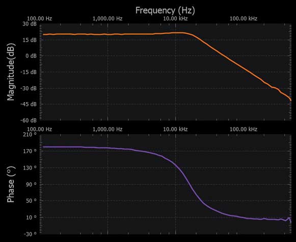
Set Channel 1 as the reference. Set the amplitude to 200 mV, 0 V offset. Under display settings, set the magnitude from –35 dB to +15 dB and the phase from
–90° to +180°. Set the sample count to 100. Turn on the power supplies and run a frequency sweep from 7.5 kHz to 1 MHz. See Figure 6.
Figure 6. Sallen-Key second-order high-pass filter frequency response.
Sallen-Key Band-pass Filter
The band-pass configuration of the Sallen-Key filter has a severe limitation. The Q value determines the gain of the filter, that is, it cannot be set independently, as it can with the low-pass or high-pass cases. The voltage gain can be computed using Equation 4.
Shown in Figure 7 is the Sallen-Key second-order band-pass filter configuration.
Set Channel 1 as the reference. Set the amplitude to 200 mV, 0 V offset. Under display settings, set the magnitude from –35 dB to +5 dB and the phase from
–180° to +180°. Set the sample count to 100. Turn on the power supplies and run a frequency sweep from 7.5 kHz to 1 MHz. See Figure 9.
Figure 9. Sallen-Key second-order band-pass filter frequency response.
It is also possible to design a Sallen-Key notch filter, but it has undesirable characteristics. The resonant frequency, or the notch frequency, cannot be adjusted easily due to component interaction. Thus, it is not included in this lab activity, although you can try simulating the Sallen-Key notch filter circuit in LTspice®.
Other Filter Configurations
State Variable Filters
A state variable filter configuration offers the most precise implementation of the filter function at the expense of many more circuit elements. All three
major parameters (gain, Q, and fr) can be adjusted independently, and low-pass, high-pass, and band-pass outputs are available simultaneously. A notch and
all-pass filter are also possible to configure using the state variable filter. With an added amplifier section summing the low-pass and high-pass sections, the notch function can also be synthesized. An all-pass filter may also be built with the four-amplifier configuration by subtracting the band-pass output from the input. Shown in Figure 10 is the state variable filter configuration that outputs a lowpass, high-pass, and band-pass frequency response.
Figure 10. State variable filter.
Tuning the resonant frequency of a state variable filter is accomplished by varying R4 and R5. While you do not have to tune both, it is preferable to vary over a wide range. By holding R1 constant, tuning R7 sets the low-pass gain and tuning R2 sets the high-pass gain. Band-pass gain and Q are set by the ratio of R3 and R7. Note that the low-pass and high-pass outputs are inverted in phase while the band-pass output maintains the phase.
Hardware Setup
Build the breadboard circuit presented in Figure 11.
Figure 11. State variable filter breadboard connection.
Procedure
Connect Channel 2 to the low-pass filter output. Set Channel 1 as the reference. Set the amplitude to 200 mV, 0 V offset. Under display settings, set the magnitude from –40 dB to +30 dB and the phase from –45° to +180°. Set the sample count to 100. Turn on the power supplies and run a frequency sweep from 100 Hz to 250 kHz. See Figure 12.
Figure 12. State variable filter, low-pass frequency response.
Now, try connecting Channel 2 to either band-pass or low-pass output and run a sweep.
Tow-Thomas Filter
Another example of a second-order active filter is the Tow-Thomas filter, sometimes referred to as a biquadratic (biquad) filter. Figure 13 shows an example of the Tow-Thomas (biquad) filter.
Figure 13. Tow-Thomas filter circuit.
The Tow-Thomas filter is tunable like the state variable (KHN) filter: Adjust R3 to change the Q factor, R4 to change the resonant frequency, and R1 to set the gain. To minimize the effects of component value interaction, adjust the resonant frequency first followed by the Q and finally the gain. The bandwidth of the Tow-Thomas filter is defined by Equation 5.
Upon closer look, the Tow-Thomas filter configuration is a minor rearrangement of the state variable filter. It has no separate high-pass output, but it generates two low-pass outputs, one in phase and one out of phase, and a band-pass output that inverts the phase. Connections of each output are shown in Figure 13. However, adding a fourth amplifier to the current filter configuration allows the filter to generate either high-pass, notch, or all-pass filters. An all-pass filter adds a phase shift response to the circuit while leaving the amplitude of the signal untouched. It has a unity gain for all frequencies.
Hardware Setup
Build the breadboard circuit presented in Figure 14. Set the positive supply to +5 V and the negative supply to –5 V.
Set the sweep as logarithmic with Channel 1 as the reference, the amplitude to 200 mV with 0 V offset, and the samples count to 75. Set the display from
–60 dB to +30 dB and from –30° to +210°. Turn on the power supplies and run a single frequency sweep from 100 Hz to 500 kHz. See Figure 15.
Figure 15. Tow-Thomas filter circuit frequency response.
Twin-T Notch Filter
The circuit shown in Figure 16 is a Twin-T notch filter. It is used as a general purpose notch (narrow band stop) circuit. Recall that a band-stop filter attenuates and blocks frequencies between its lower and higher cut-off frequencies.
Figure 16. Twin-T notch filter circuit.
The Twin-T notch filter circuit is comprised of two T-shaped networks: A RCR T-network and a CRC T-network. Resistors R1 and R2 with capacitor C3 form
the RCR T-network, while capacitors C1 and C2, alongside with resistor R3 form the CRC T-network. The design configurations are shown in Equation 6 and Equation 7.
Take note of the values of R and C. They determine the center notch frequency fo of the filter, which is defined by the expression in Equation 8.
In its passive implementation, the Twin-T notch filter has its Q fixed at 0.25. Implementing positive feedback to the reference node can fix the problem. This is done by setting up a voltage divider using R4 and R5 at the output of the filter and connect it to a voltage follower. Then the output of the voltage follower is supplied back to the junction of R3 and C3.
The signal feedback is given by the resistors R4 and R5 determine the Q of the filter as well as the notch depth. The quality factor is defined by Equation 9.
To achieve the maximum notch depth, eliminate resistors R4 and R5 alongside the op amp connected to them and connect the junction between R3 and C3 junction
directly to the output.
Hardware Setup
On your breadboard, build the circuit in Figure 17. Use the positive and negative supplies of the ADALM2000. Figure 18 replaces R4 and R5 with a potentiometer allowing more control for the Q of the circuit.
Figure 18. Twin-T notch filter circuit with potentiometer breadboard connection.
Procedure
Set the sweep as logarithmic with Channel 1 as the reference, the amplitude to 200 mV with 0 V offset, and the samples count to 100. Set the display from –25 dB to +5 dB and –140° to +80°. Turn on the +5 V and –5 V power supplies and sweep from 30 kHz to 300 kHz. See Figure 19.
Figure 19. Twin-T notch filter circuit frequency response.
Your circuit’s frequency response should be similar to your simulation result.
Question
Considering the circuit in Figure 1, change the gain of the amplifier by replacing the values of R3 and R4. What do you observe with the frequency response?
Antoniu Miclaus is a software engineer at Analog Devices, where he works on embedded software for Linux and no-OS drivers, as well as ADI academic programs, QA automation, and process management. He started working at ADI in February 2017 in Cluj-Napoca, Romania. He holds an M.Sc. degree in software engineering from the Babes-Bolyai University and a B.Eng. degree in electronics and telecommunications from the Technical University of Cluj-Napoca.
Doug Mercer
Doug Mercer received his B.S.E.E. degree from Rensselaer Polytechnic Institute (RPI) in 1977. Since joining Analog Devices in 1977, he has contributed directly or indirectly to more than 30 data converter products and holds 13 patents. He was appointed to the position of ADI Fellow in 1995. In 2009, he transitioned from full-time work and has continued consulting at ADI as a fellow emeritus contributing to the Active Learning Program. In 2016, he was named engineer in residence within the ECSE department at RPI.