Objective
The objective of this exercise is to explore the use of complementary MOS transistors as an analog voltage switch.
Concept
The ideal analog switch has no on-resistance, infinite off-impedance, and zero-time delay, and can handle large signal and common-mode voltages. Real analog switches made with MOS transistors meet none of these criteria, but if we understand the limitations of analog switches, most of these limitations can be overcome. The on-resistance is one of these limitations, and this lab activity will attempt to characterize this switch specification.
Materials
- ADALM2000 Active Learning Module
- Solderless breadboard
- Jumper wires
- One CD4007 CMOS transistor array
- Two NPN transistors (2N3904 or equivalent)
- One 4.7 kΩ resistor


NMOS Directions
Construct the test circuit shown in Figure 2. The blue boxes indicate connections to the connector on the ADALM2000. NMOS and PMOS devices M1 and M2 are contained in the CD4007 package. All unused pins can be left floating. To measure the on-resistance (RON) of the MOS transistors we first need to force a known current through the resistance and then measure the voltage across the resistance. The two NPN devices Q1 and Q2 along with resistor R1 form a current source with an output current of approximately 1 mA. The exact magnitude of this current is not important in that we are mainly interested in the change in the RON of the MOS devices as the voltage at their source/drain varies over the range of between the plus and minus power supplies.
In this first test, only NMOS device M1 is turned on and PMOS device M2 is turned off.


Hardware Setup
Connect the circuit shown in Figure 2 to a breadboard.


Procedure
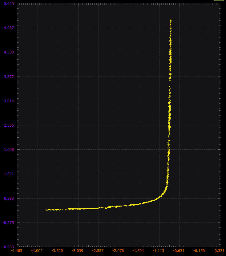
Configure waveform generator 1 as a 100 Hz triangle wave with an amplitude of 9 V peak-to-peak and an offset of 500 mV. This will swing the voltage on the NMOS switch transistor from +5 V to –4 V. We cannot swing the voltage all the way to –5 V because of the NPN current source Q2. Be sure to turn on the external user power supplies (Vp and Vn) before running the waveform generator. Configure the scope screen in XY mode with Channel 1 on the x-axis, and Channel 2 (the voltage across the switch) on the y-axis. Use the math function to calculate the resistance (C2 / 1 mA). Note: You can get a more precise estimate of the current source by measuring the voltage across R1 and its actual resistance.
Configure the oscilloscope instrument to capture several periods of the two signals being measured. An XY plot example using Scopy is presented in Figure 4.

PMOS Directions
Now modify your circuit to look like Figure 5 by connecting the gates of both M1 and M2 to the negative power supply Vn. In this second test, only PMOS device M2 is turned on and NMOS device M1 is turned off.


Hardware Setup
Connect the circuit shown in Figure 5 to a breadboard.


Procedure
Repeat the sweep of the voltage from the previous section and plot the on-resistance of just the PMOS transistor.
Configure the oscilloscope instrument to capture several periods of the two signals being measured. An XY plot example using Scopy is presented in Figure 7.


CMOS Directions
Now modify your circuit to look like Figure 8 by connecting the gate of M1 to the positive power supply Vp and the gate of M2 to the negative power supply Vn. In this last test, both NMOS device M1 and PMOS device M2 are turned on.


Hardware Setup
Connect the circuit shown in Figure 8 to a breadboard.


Procedure
Repeat the sweep of the voltage from the previous section and plot the on-resistance of the combined NMOS and PMOS transistors.
Configure the oscilloscope instrument to capture several periods of the two signals being measured. An XY plot example using Scopy is presented in Figure 10.


Questions:
- For the circuit in Figure 2, at what voltage does the NMOS device turn off?
- For the circuit in Figure 2, what happens to the drain-to-source voltage as the NMOS transistor turns off?
- For the circuit in Figure 5, at what voltage does the PMOS device turn off?
- For the circuit in Figure 5, what happens to the source-to-drain voltage as the PMOS transistor turns off?
You can find the answers at the StudentZone blog.

