Simple NPN Diode Connection
Objective:
The purpose of this activity is to investigate the forward and reverse current vs. voltage characteristics of a bipolar junction transistor (BJT) connected as a diode.
Materials:
- ADALM2000 active learning module
- Solderless breadboard
- One 1 kΩ resistor (or any similar value)
- One small signal NPN transistor (2N3904)
Directions:
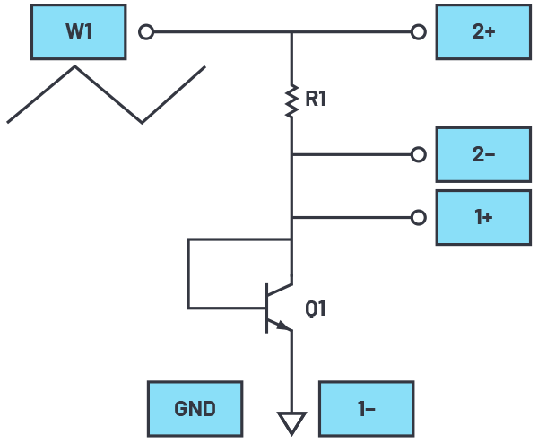
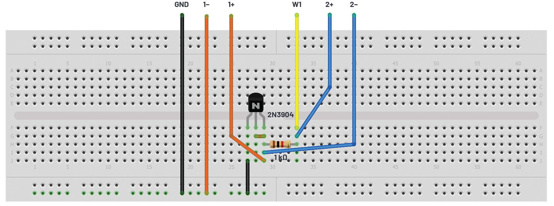
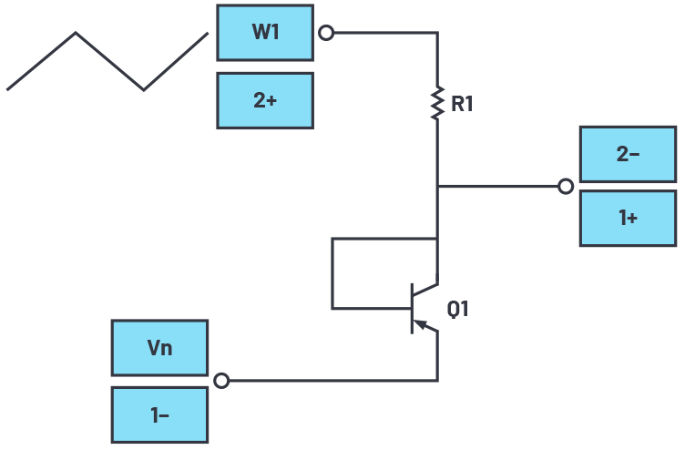
The current vs. voltage characteristics of the emitter-base junction of an NPN transistor can be measured using the ADALM2000 lab hardware and the following connections. Set up the breadboard with waveform generator W1 attached to one end of resistor R1. Also connect Scope Input 2+ here. Connect the base and collector of Q1 to the opposite end of R1 as shown in the diagram. The emitter of Q1 is connected to the ground. Connect Scope Input 2– and Scope Input 1+ to the base-collector node of Q1. Scope Input 1– can be optionally grounded as well.

Hardware Setup:
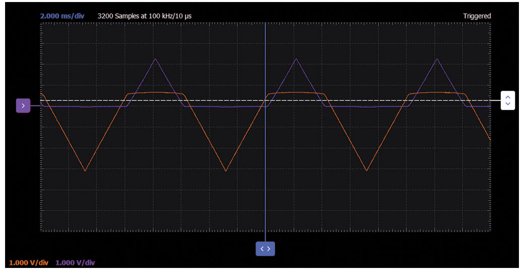
The waveform generator should be configured for a 100 Hz triangle wave with 6 V amplitude peak-to-peak and 0 V offset. The differential Scope Channel 2 (2+, 2–) measures the current in the resistor (and in the transistor). Scope Channel 1 (1+) is connected to measure the voltage across the diode connected transistor. The current flowing through the transistor is the voltage difference 2+ and 2– divided by the resistor value (1 kΩ).

Procedure:
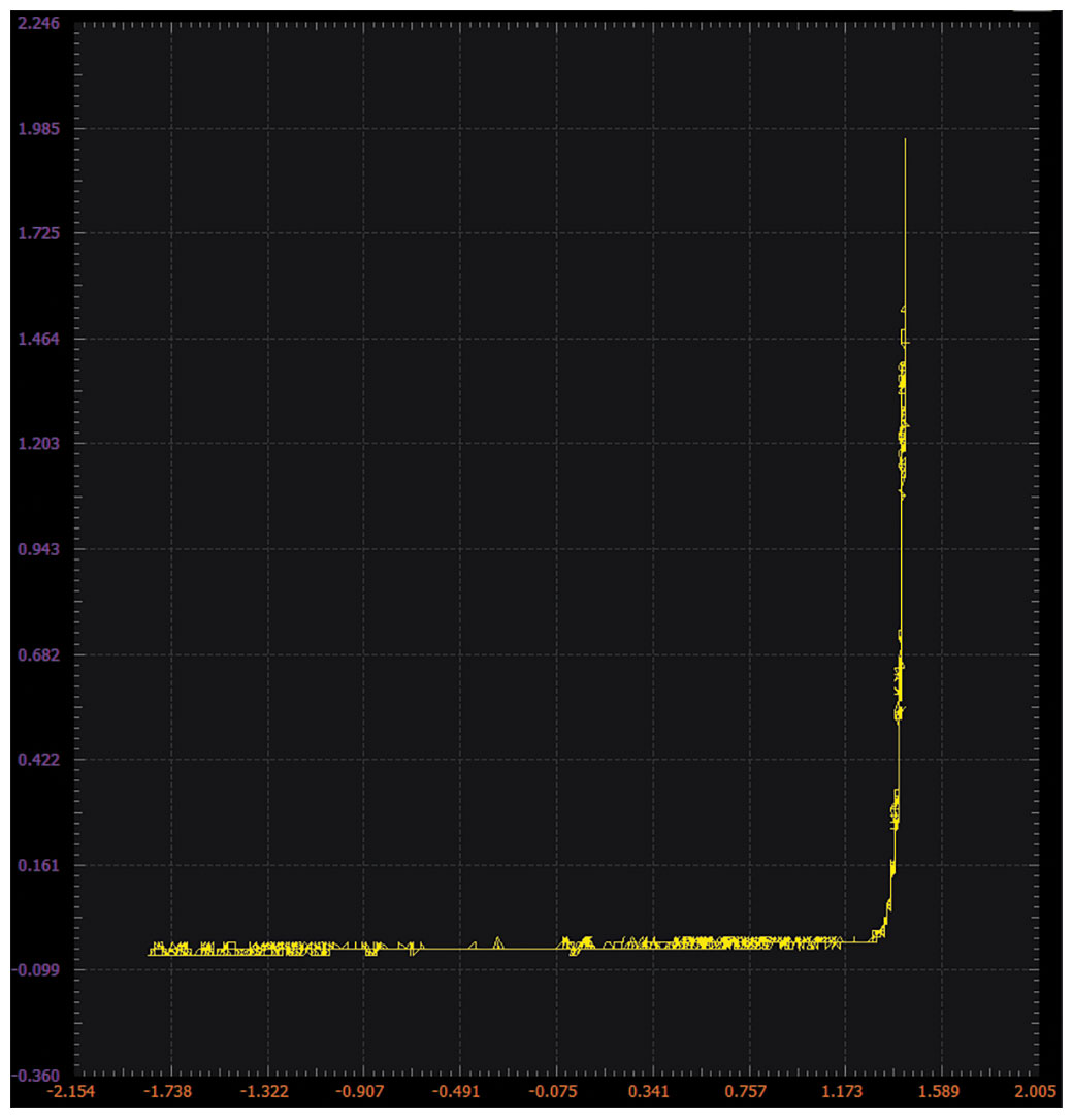
Load the captured data into a spreadsheet program and calculate the current. Plot the current vs. the voltage across the transistor (VBE). No current flows in the reverse direction. In the forward conduction region, the voltage-current relationship is logarithmic. If the current is plotted on a log scale, the line should be straight.


Reverse Breakdown Characteristics
Objective:
The purpose of this activity is to investigate the reverse break down voltage characteristics of the emitter base junction of a BJT connected as a diode.
Materials:
- One 100 Ω resistor
- One small signal PNP transistor (2N3906)
Directions:
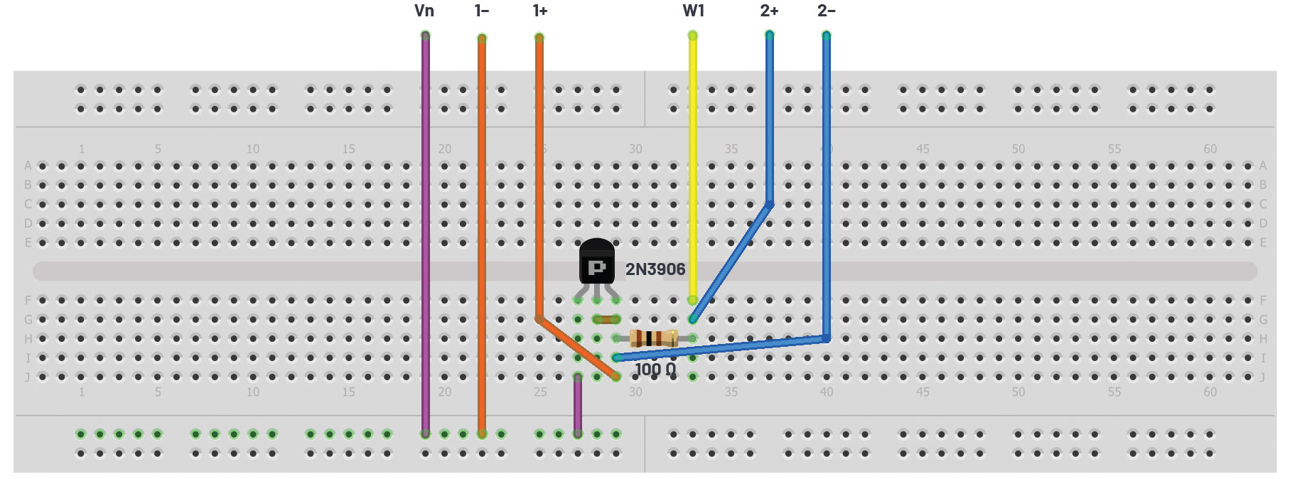
Set up the breadboard with the waveform generator output attached to one end of the series connected resistor 100 Ω R1 and the base and the collector of Q1 as shown in Figure 2. The emitter is connected to the –5 V fixed power supply. Scope Channel 1 (1+) is connected to the base-collector node while 1– is connected to the emitter node. Scope Channel 2 measures the voltage across R1 and thus measures the current through Q1. The PNP 2N3906 is chosen over the NPN 2N3904 because the PNP emitter-base breakdown voltage is less than the +10 V max that can be generated using the ADALM2000 while the NPN’s is likely to be higher than 10 V.

Hardware Setup:
The waveform generator should be configured for a 100 Hz triangle wave with 10 V amplitude peak-to-peak and 0 V offset. Scope Channel 1 (1+) is used to measure the voltage across the transistor. The setup should be configured with Channel 2 connected across resistor R1 (2+, 2–). Both channels should be set to 1 V per division. The current flowing through the transistor is the voltage difference between 2+ and 2– divided by the resistor value (100 Ω).

Procedure:
The lab hardware power supplies limit the maximum voltage available to less than 10 V. The emitter-base reverse breakdown voltage of many transistors is larger than this. In the configuration shown in Figure 6, voltages between 0 V and 10 V (W1 peak-to-peak swing) can be measured.

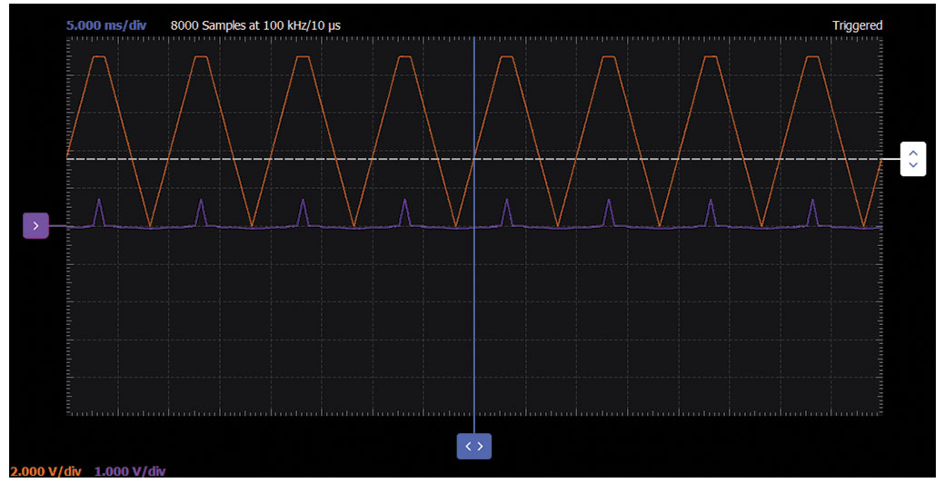
Capture the scope waveforms and export them into a spreadsheet program. For the 2N3906 PNP used in the example , the breakdown voltage of the emitter-base junction is around 8.5 V.
Lowering the Effective Forward Voltage of the Diode
Objective:
The purpose of this activity is to investigate a circuit configuration with smaller forward voltage characteristics than that of a BJT connected as a diode.
Materials:
- One 1 kΩ resistor
- One 150 kΩ resistor (or 100 kΩ in series with 47 kΩ)
- One small signal NPN transistor (2N3904)
- One small signal PNP transistor (2N3906)
Directions:
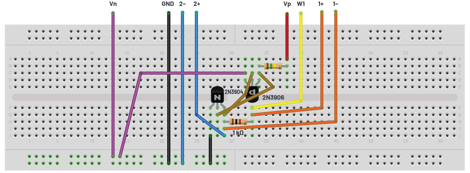
Set up the breadboard with waveform generator W1 attached to one end of the series connected resistor R1 and collector of NPN Q1 and the base of PNP Q2 as shown in Figure 8. The emitter of Q1 is connected to ground. The collector of Q2 is connected to Vn (-5 V). The first end of resistor R2 is connected to Vp (+5 V). The second end of R2 is connected to the base of Q1 and the emitter of Q2. The single-ended input of Scope Channel 2 (2+) is connected to the collector of Q1.


Hardware Setup:
The waveform generator should be configured for a 100 Hz triangle wave with 8 V amplitude peak-to-peak and 2 V offset. Scope Channel 2 (2+) is used to measure the voltage across the transistor. The current flowing through the transistor is the voltage difference between scope input 1+ and 1– divided by the resistor value (1 kΩ).

Procedure:
The turn-on voltage of the diode is now about 100 mV compared to 650 mV for the simple diode connection in the first example. Plot the VBE of Q1 as W1 is swept.

VBE Multiplier Circuit
Objective:
Now that we have seen a way to make VBE effectively smaller, the purpose of this activity is to make VBE larger and showcase characteristics of a larger forward voltage compared to those of a single BJT connected as a diode.
Materials:
- Two 2.2 kΩ resistors
- One 1 kΩ resistor
- One 5 kΩ variable resistor, potentiometer
- One small signal NPN transistor (2N3904)
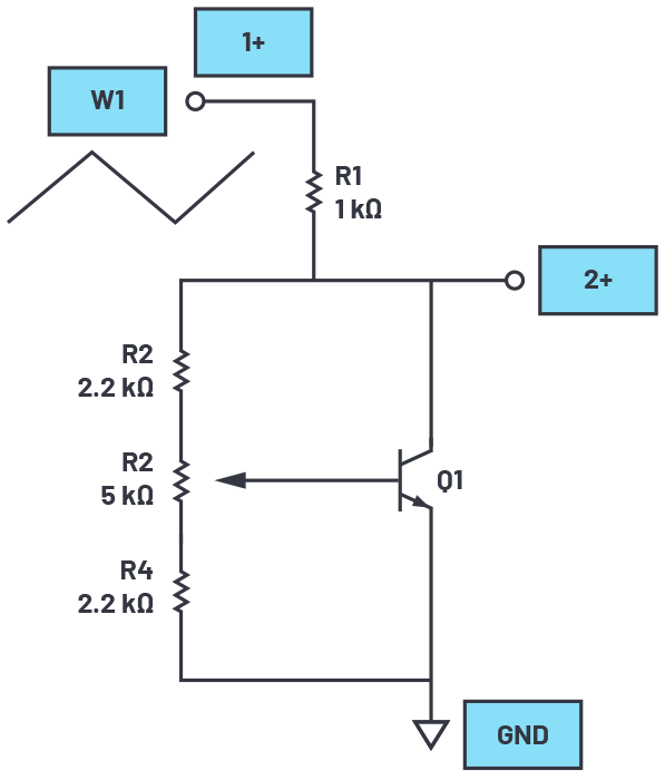
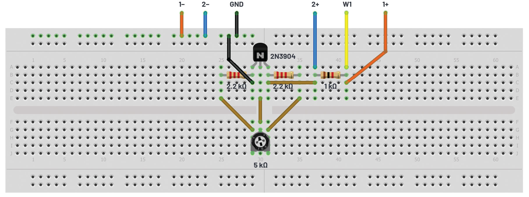
Directions:
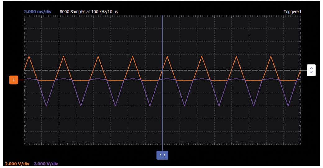
Set up the breadboard with waveform generator W1 attached to one end of resistor R1, as indicated in Figure 11. The emitter of Q1 is connected to the ground. Resistors R2, R3, and R4 form a voltage divider with the wiper of potentiometer R3 connected to the base of Q1. The collector of Q1 is connected to the second end of R1 and the top of the voltage divider at R2. Scope Channel 2 (2+) is connected to the collector of Q1.

Hardware Setup:
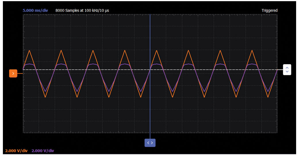
The waveform generator should be configured for a 100 Hz triangle wave with 4 V amplitude peak-to-peak and 2 V offset. The single-ended input of Scope Channel 2+ is used to measure the voltage across the transistor. The setup should be configured with Channel 1+ connected to display the output of generator W1 and Channel 2+ connected to display the collector voltage of Q1. The current flowing through the transistor is the voltage difference between the W1 measured by Scope Input 1+ and Scope Input 2+ divided by the resistor value (1 kΩ).

Procedure:
Starting with the potentiometer R3 set at the middle of its range, the voltage at the collector of Q2 should be about 2 times VBE. With R3 set to its minimum, the voltage at the collector should be 9/2 (or 4.5) times VBE. With R3 set to its maximum, the voltage at the collector should be 9/7 times VBE.

Questions:
- How does the voltage vs. current characteristics of this VBE multiplier compare to those of a simple diode connected transistor?
You can find the answers at the StudentZone blog.

