Objective
The objective of this lab activity is to investigate ways to produce negative reference voltages. Positive voltage references or regulator configurations are more commonly available. Conventional methods of generating a negative reference voltage from a positive voltage involve inverting op amp stages, which tend to rely on precision matched resistors for accuracy.
Background
In Figure 1a, the simple Zener diode circuit, consisting of RZ and DZ from the Zener diode regulator lab activity is used to produce a positive reference voltage, +VREF. In a positive voltage reference, a noninverting op amp buffer is often included to scale the output voltage and supply any current needed in the load. The obvious method for generating a negative reference voltage is to instead use an inverting op amp stage. The op amp inverts the +VREF and provides at the op amp output a –VREF. This approach requires two precision resistors, R1 and R2. Matching the errors of these two resistors (for example, different accuracy and different temperature coefficient), in addition to the voltage offset in the op amp, will produce an error at the output of the op amp (+VREF), which is shown in Figure 1a. However, one potential side benefit of this inverting amplifier configuration is that –VREF need not have the same absolute value as +VREF. The negative reference voltage can be scaled up or down by altering the ratio of R1 and R2. An alternate configuration we will be investigating in this lab activity is shown in Figure 1b. It generates a negative reference voltage without the dependence on ratio matched resistors, potentially providing higher accuracy with fewer components.


By examining Figure 1a, we see that, by the virtual ground nature of the inverting op amp configuration, the Zener voltage +VREF is impressed across resistor R1. If R2 is exactly equal to R1, this same voltage VREF will also appear across R2 but with the sign reversed with respect to ground. Since the voltage across R2 is the same as that across the Zener diode, we can in effect replace R2 with the diode in the feedback loop as in Figure 1b and still produce the same voltage at –VREF. RZ simply sets the bias current level in the Zener much as RZ in Figure 1a. In Figure 1b, IZ is equal to VDD/RZ, whereas in Figure 1a, IZ is equal to (VDD – +VREF)/RZ. To design for the same IZ in both cases, we simply change the value of RZ. Capacitor C1 decouples the reference diode between its ground and output terminals. In addition, low inductance 0.1 μF supply decoupling capacitors (not shown in Figure 1) are often connected to +VDD and –VSS very close to the op amp.
Circuit Description
In theory, this circuit can be built using almost any three-terminal voltage reference circuit and a low noise, low offset operational amplifier. To build a negative reference based on the band-gap concept, we would require high quality PNP transistors and the PNPs generally available in IC processes are not as high quality as the available NPN devices. These NPN-based band-gap circuits will provide a couple of examples we can use to explore this negative reference configuration. The first circuit iteration in Step 1 of this lab will use a diode as a reference and further iterations will substitute NPN transistor-based two-terminal (shunt) and three-terminal (series) circuits as the reference element.
Materials
- ADALM2000 Active Learning Module
- Solderless breadboard and jumper wire kit
- One 4.7 kΩ resistor
- Two 1.5 kΩ resistors
- Two 20 kΩ resistors
- One 2.2 kΩ resistor
- One 100 Ω resistor
- One 10 kΩ variable resistor (potentiometer)
- Four small signal NPN transistors (2N3904 and SSM2212)
- Two LEDs (any color will do)
- One OP482 or OP484 quad op amp
- One 1 nF capacitor
- Two 0.01 μF capacitors
- Two 0.1 μF capacitors (supply decoupling capacitors for +5 V and –5 V supplies)
Step 1
The Zener diode (1N4735) supplied in the ADALP2000 Analog Parts Kit is a 6.1 V diode. 6.1 V is much too high a reverse breakdown voltage to build this circuit using the fixed ±5 V power supplies of the ADALM2000 hardware. The forward voltage of an LED is in the range of 1.6 V to 2.0 V depending on the color of the diode. While not a proper reference diode, we can build the circuit for instructional purposes using the LEDs from the ADALP2000 Analog Parts Kit.
Build both versions of the circuits in Figure 1a and Figure 1b as shown in Figure 2 on your solderless breadboard. Use two LEDs preferably of the same color. Green LEDs will have a higher forward voltage drop than red or yellow. We want the diode current, ID, to be about 1 mA. The current ID should be close to the same value in both versions of the circuit (see figures 1a and 1b). In Case a, ID will be (+5 V – VD)/R3. In Case b, ID will be +5 V/R4, so a 4.7 kΩ resistor would give about 1 mA. If we use 2 V as an estimate for VD, then R3 would be around 3 kΩ. You can get 3 kΩ by connecting two 1.5 kΩ resistors from the parts kit in series. Also, for Case a, we need to pick values for R1 and R2. We want the current in R1 to be much smaller than the current in R3. So, setting R1 and R2 to a much higher value such as 20 kΩ should satisfy that condition.


Hardware Setup
Open the voltage supply control and the voltmeter instrument windows from the Scopy software. A DMM, if available, could be useful to measure the DC voltages more accurately in the circuit than the Scopy voltmeter instrument. Breadboard connections are presented in Figure 3.
Procedure
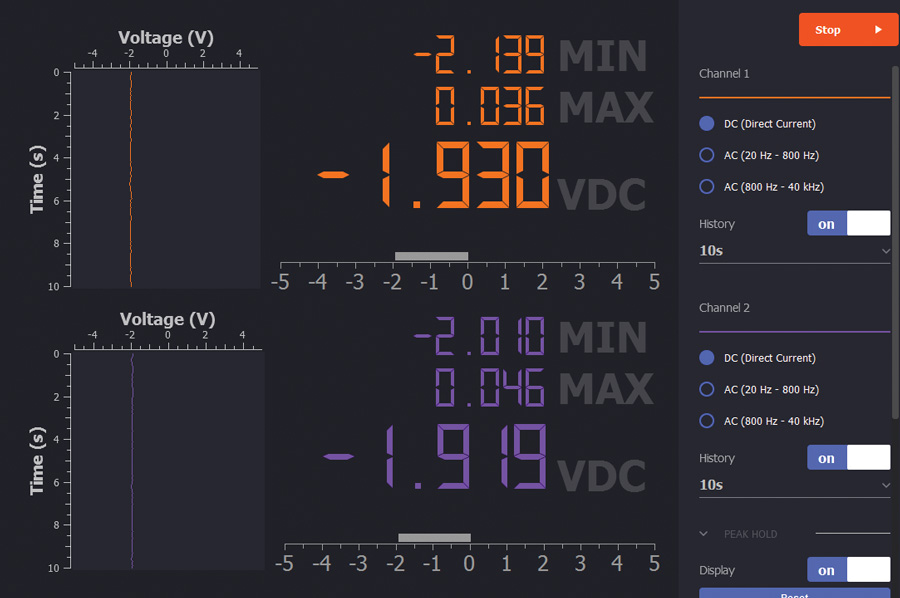
Turn on both the positive and negative power supplies. Observe the two voltages at –VREF, pins 8 and 14 of the op amp, and at +VREF on the LED.


Step 2
Modify your breadboard setup from Step 1 as shown in Figure 5. Be sure to turn off the power supplies before making any modifications to your breadboard. Replace the LED with the shunt regulator stage. Resistors R1 and R2 as well as transistor Q1 are connected as the zero-gain amplifier. Resistor R3 and transistor Q2 are added as in the stabilized current source. If the SSM2212 matched NPN pair is used, it should be used for devices Q1 and Q2. Q3 is added as the common emitter stage, its base connected to the collector of Q2, and the collector connected to the combined node of R1, R3, and R4.


Hardware Setup
The setup is the same in Step 1. Breadboard connections are presented in Figure 6.
Procedure
Turn on both the positive and negative power supplies. Observe the voltage at –VREF, Pin 14 of the op amp, and across the band-gap shunt regulator (collector and emitter of Q3). You can adjust potentiometer R3 to produce a –1.25 V reference voltage.
Testing Supply Headroom
To test the headroom requirements for +VDD, disconnect the fixed positive power supply from +VDD and remove any supply decoupling capacitors. Be sure to turn off the power supplies before making any changes or additions to your breadboard. Now connect +VDD to AWG 1. Set AWG 1 to trapezium (trapezoid) waveform at 100 Hz. Set the amplitude to 5 V peak-to-peak with a 2.5 V offset for a 0 V to +5 V swing. Connect Scope Channel 1 to the output of AWG1 and connect Scope Channel 2 to –VREF of the first example circuit at Pin 14 of the OP482. Use the oscilloscope instrument in the XY mode, scope channel for X, and Scope Channel 2 for Y. Start AWG 1 and turn on the fixed negative 5 V power supply. Record the minimum +VDD voltage where –VREF starts to remain constant at –1.25 V.
To test the headroom requirements for –VSS, reconnect +VDD to the fixed positive power supply. Disconnect the fixed negative power supply from –VSS and remove any supply decoupling capacitors. Now connect –VSS to AWG 1. Set the amplitude to 5 V peak to peak with a –2.5 V offset for a 0 to –5 V swing. Start AWG 1 and turn on the fixed positive 5 V power supply. Repeat your measurements of Pin 14 of the OP482, recording the lowest value for –VSS where the reference voltage is constant.


Step 3
Modify your breadboard setup from Step 1 as shown in Figure 7. Be sure to turn off the power supplies before making any modifications to your breadboard. Change the two-terminal, shunt, regulator used in Step 2 to the three-terminal reference by adding emitter follower stage Q4 and compensation capacitor C1.


Hardware Setup
The setup is the same in Step 1. Breadboard connections are presented in Figure 7.
Procedure
Turn on both the positive and negative power supplies. Observe the voltage at –VREF, Pin 14 of the op amp, and across the band-gap three-terminal regulator (emitter of Q4 and emitter of Q3).


Question:
For the circuits in Figure 2, what happens with the output voltage reference value if the green LEDs are replaced with red or yellow LEDs?
You can find the answer at the StudentZone blog.

