Objective
The purpose of this lab activity is to explore the concepts of analog-to-digital conversion by building explanatory examples.
Background
Analog-to-digital converters (ADCs) translate analog signals—real-world signals like temperature, pressure, voltage, current, distance, or light intensity—into a digital representation of that signal. This digital representation can then be processed, manipulated, computed, transmitted, or stored.


An ADC samples an analog waveform at uniform time intervals and assigns a digital value to each sample. The digital value appears on the converter’s output in a binary coded format. The value is obtained by dividing the sampled analog input voltage by the reference voltage and then multiplying by the number of digital codes. The resolution of the converter is set by the number of binary bits in the output code.


An ADC carries out two processes: sampling and quantization. The ADC represents an analog signal, which has infinite resolution, as a digital code that has finite resolution. The ADC produces 2N digital values where N represents the number of binary output bits. The analog input signal will fall between the quantization levels because the converter has finite resolution, which results in an inherent uncertainty or quantization error. That error determines the maximum dynamic range of the converter.


The sampling process represents a continuous-time domain signal with values measured at discrete and uniform time intervals. This process determines the maximum bandwidth of the sampled signal in accordance with the Nyquist theorem. This theory states that the signal frequency must be less than or equal to one-half the sampling frequency to prevent aliasing. Aliasing is a condition in which frequency signals outside the desired signal band will, through the sampling process, appear within the bandwidth of interest. However, this aliasing process can be exploited in communications systems design to downconvert a high frequency signal to a lower frequency. This technique is known as undersampling. A criterion for undersampling is that the ADC has sufficient input bandwidth and dynamic range to acquire the highest frequency signal of interest.


Sampling and quantization are important concepts because they establish the performance limits of an ideal ADC. In an ideal ADC, the code transitions are exactly 1 least significant bit (LSB) apart. So, for an N-bit ADC, there are 2N codes and 1 LSB = FS/2N, where FS is the full-scale analog input voltage. However, ADC operation in the real world is also affected by nonideal effects, which produce errors beyond those dictated by converter resolution and sample rate. These errors are reflected in a number of AC and DC performance specifications associated with ADCs.


Materials
- ADALM2000 Active Learning Module
- Solderless breadboard and jumper wire kit
- One OP482 operational amplifier
- Two AD654 voltage-to-frequency converters
- Three 1 kΩ resistors
- Five 10 kΩ resistors
- One 1 nF capacitor
- One SN74HC08 AND gate
- One SN74HC32 OR gate
- One SN74HC04 inverter
- One 1 μF capacitor
- One AD7920 12-bit ADC
Flash ADC
Background
Flash ADCs, also known as parallel ADCs, are one of the fastest ways to convert an analog signal to a digital signal. Flash ADCs are ideal for applications requiring very large bandwidth, but they consume more power than other ADC architectures and are generally limited to 8-bit resolution. Typical examples include data acquisition, satellite communication, radar processing, sampling oscilloscopes, and high density disk drives.
Flash ADCs are made by cascading high speed comparators. For an N-bit converter, the circuit employs 2N -1comparators, while 2N resistors provide the reference voltage. Each comparator produces a 1 when its analog input voltage is higher than the reference voltage applied to it. Otherwise, the comparator output is 0. The point where the code changes from ones to zeros is the point at which the input signal becomes smaller than the respective comparator reference-voltage levels.
Consider the circuit presented in Figure 6.


The circuit represents the analog side of a 2-bit flash ADC with the architecture known as thermometer code (unary code) encoding. For this type of circuit, additional logical circuitry is used to decode the unary code to appropriate digital output code. Using logic AND, OR, and INV gates we can build a priority encoder. Its output is the binary representation of the original number starting from zero of the most significant input bit.


As mentioned before, flash ADCs are made using high speed comparators, but for convenience, we are going to use the OP482 quad op amp to illustrate the principle. Alternatively, you can build the circuit using four AD8561 comparators.
Hardware Setup
Build the circuit presented in Figure 7 on your solderless breadboard. This is a circuit for a 2-bit flash ADC with encoded output.
Procedure
Supply the circuit to ±5 V from the power supply. Configure AWG1 of the Signal Generator in Scopy to Rising Ramp Sawtooth with 5 V amplitude peak-to-peak, 2.5 V offset, and 100 Hz frequency. Use AWG2 as 5 V constant reference voltage for the ADC.
Configure the Logic Analyzer so that the digital channels DIO0, DIO1, and DIO2 form a channel group decoded for unary code and channels DIO6 and DIO7 form a channel group decoded for parallel output.
A plot with the output signals is presented in Figure 9.

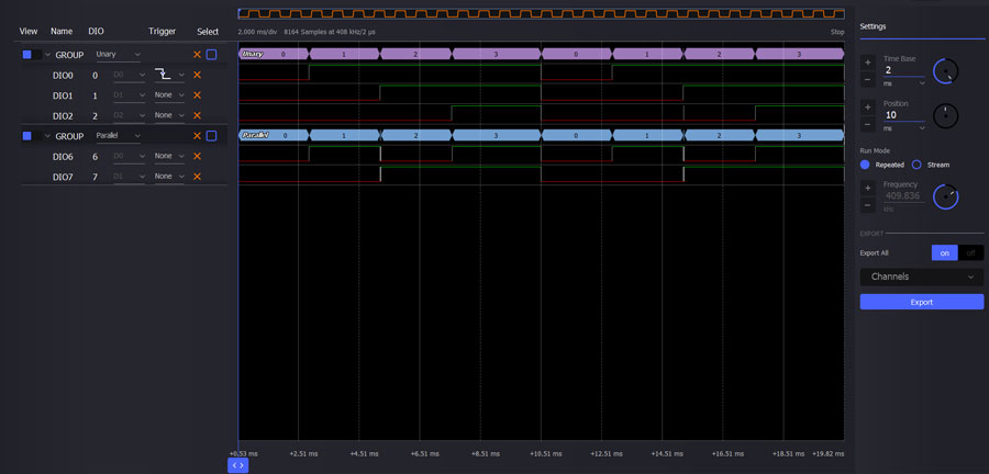
The unary group channel represents the output thermometer code for the 2-bit flash ADC with all possible output values, by varying the input analog voltage through the entire available range (0 V to 5 V). On the parallel channel are represented the binary values equivalent to the ADC output states.
Voltage-to-Frequency Converter as ADC
Background
For this particular application, the AD654 voltage-to-frequency converter is used as an ADC.


In order to achieve the conversion, the output of the converter should be connected to a microcomputer that has an interval timer/event counter.
The total number of signal edges (rising or falling) counted during the count period is proportional to the input voltage. For this particular setup, a 1 V full-scale input voltage produces a 100 kHz signal. If the count period is 100 ms, then the total count will be 10,000. Scaling from this maximum is then used to determine the input voltage. Thus, a count of 5000 corresponds to an input voltage of 0.5 V.
Hardware Setup
Build the breadboard circuit for using a voltage-to-frequency converter as an ADC, as shown in Figure 11.
Procedure
Supply the circuit to 5 V from the power supply. Configure AWG1 of the Signal Generator to 1 V constant voltage.
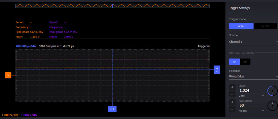
Configure the scope such that the output signal is displayed on Channel 1, and enable the frequency measurement from the Channel 1 Measure tab. A plot with the output signal is presented in Figure 12.


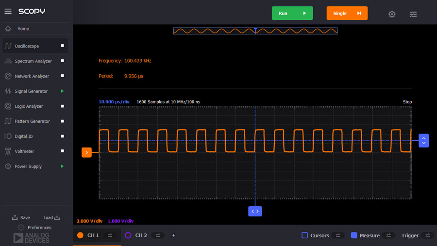
The plot in Figure 12 represents the output signal of the voltage-to-frequency converter for a 1 V full-scale input voltage. Notice that the corresponding output frequency is 100 kHz.
Now set the input voltage at 0.5 V. A plot with the output signal is presented in Figure 13.

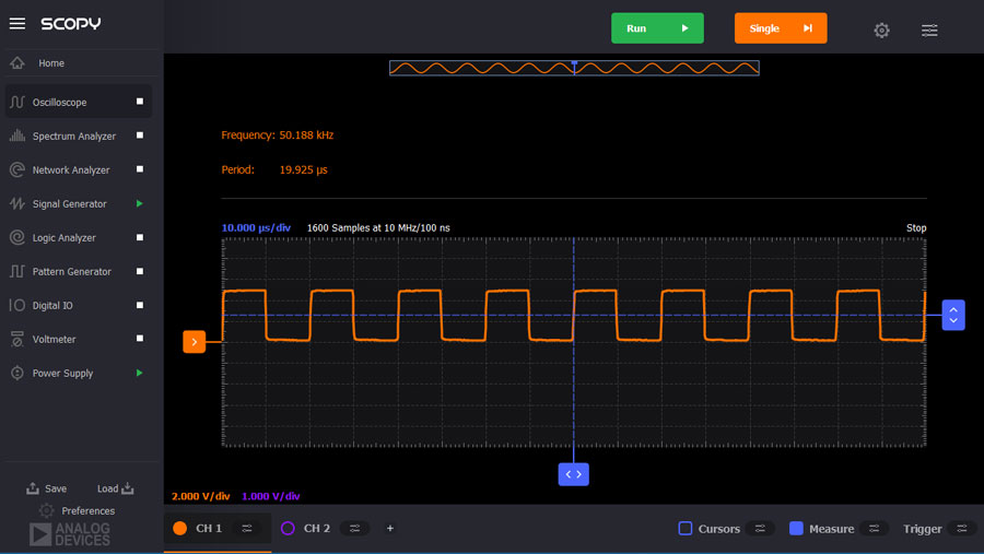
The plot represents the output signal of the voltage-to-frequency converter for a 0.5 V half-scale input voltage. Note that the output frequency is now 50 kHz.
Successive Approximation Register (SAR) ADC
Background
The successive approximation register (SAR) ADC converts the continuous analog waveform into a discrete digital representation via a binary search through all possible quantization levels before finally converging upon a digital output for each conversion.
Usually, the SAR ADC circuit consists of four subcircuits:
- Sample-and-hold circuit (S/H) to acquire the input voltage (VIN).
- Analog voltage comparator that compares VIN to the output of the internal DAC and outputs the result of the comparison to the SAR.
- SAR subcircuit designed to supply an approximate digital code of VIN to the internal DAC.
- Internal reference DAC that supplies the comparator with an analog voltage equal to the digital code output of the SAR.


The SAR is initialized so that the most significant bit (MSB) is equal to a digital 1. This code is fed into the DAC, which then supplies the analog equivalent of this digital code (VREF/2) into the comparator circuit for comparison with the sampled input voltage. If this analog voltage exceeds VIN, the comparator causes the SAR to reset this bit; otherwise, the bit is left at 1. Then the next bit is set to 1 and the same test is done, continuing this binary search until every bit in the SAR has been tested. The resulting code is the digital approximation of the sampled input voltage and is finally output by the SAR at the end of the conversion (EOC).


Figure 15 shows an example of a 4-bit conversion. The y-axis represents the DAC output voltage. In the example, the first comparison shows that VIN < VDAC. Thus, Bit 3 is set to 0. The DAC is then set to 0100 and the second comparison is performed. As VIN > VDAC, Bit 2 remains at 1. The DAC is then set to 0110, and the third comparison is performed. Bit 1 is set to 0, and the DAC is then set to 0101 for the final comparison. Finally, Bit 0 remains at 1 because VIN > VDAC.
Hardware Setup
In order to emphasize the operation principle of the SAR ADC with the ADALM2000, we will use for the DAC part the circuit that will be studied in the next activity, but for this setup we will use a 4-bit DAC (instead of an 8-bit). The output of the DAC will be connected to a comparator, while the SAR will be simulated via a script that performs the binary search based on the comparator’s output and generates the proper binary value.


Build the breadboard circuit for a SAR ADC, as shown in Figure 17.


Two precision rail-to-rail op amps from the OP484 integrated circuit were used for the SAR ADC—one is used for the R-2R ladder DAC, and the other one as comparator between the DAC output and input voltage.
Procedure
Supply the circuit to ±5 V from the power supply. Configure the scope so that the comparator output signal is displayed on Channel 1 and the DAC output on Channel 2.
Group the first four digital channels in the Logic Analyzer and set the decoder to parallel.
Download the SAR ADC script and run it using the Scopy interface.
The digital code is updated using the successive approximation method based on the feedback received from the comparator output.
Visualize the approximation behavior of the DAC output in time domain using the Oscilloscope. A plot example is presented in Figure 18.

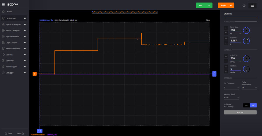
The output value will try to reach the input value (set to 2 V) after several approximation steps.
AD7920 12-Bit ADC
Background
The AD7920 is a 12-bit high speed, low power, SAR ADC. It can operate with a single power supply in the range of 2.35 V to 5.25 V. This ADC can be serial interfaced. The serial clock provides the conversion clock and controls the transfer of information from the AD7920 during conversion. The conversion process and data acquisition are controlled using /CS and the serial clock, allowing the devices to interface with microprocessors or DSPs. The input signal is sampled on the falling edge of /CS, and the conversion is initiated at this point. Figure 19 shows simplified schematics of the ADC during the acquisition and the conversion phase.
The acquisition phase is when SW2 is closed and SW1 is in Position A. With this setup, the comparator is held in a balanced condition, and the sampling capacitor acquires the signal on VIN. For the ADC to start a conversion, SW2 opens and SW1 moves to Position B causing the comparator to become unbalanced. The control logic and charge redistribution DAC are used to add and subtract fixed amounts of charge from the sampling capacitor to bring the comparator back to a balanced condition, so the conversion is completed.
Hardware Setup
Figure 21 shows a typical connection setup for the AD7920. VREF is taken internally from VDD so it should be well decoupled. This provides an analog input range of 0 V to VDD. The conversion result is output in a 16-bit word with four leading zeros followed by the MSB of the 12-bit or 10-bit result.


Procedure
Open Scopy and enable the positive power supply to 3 V. Configure Channel 1 of the Signal Generator as a Constant with a value in the range of 0 V to 3 V—for example, the middle domain value 1.5 V. You can monitor the actual value of these voltages on the oscilloscope.

In the Logic Analyzer, configure DIO0, DIO1, and DIO2 as a group channel. Set the group channel as SPI and the channels to corresponding SPI signals—DIO0 as CS#, DIO1 as CLK, and DIO2 as MISO. As the CS# falling edge initiates the data transfer, you should set the trigger of DIO0 to falling edge. Set the DIO1 trigger to low and from trigger settings set Trigger Logic to AND. DIO2 does not need a trigger setting as it is the output signal of the ADC. Enable the Logic Analyzer and it should be waiting for the trigger signals.
In the Pattern Generator, configure the clock signal. Enable DIO1 channel, set its Pattern as Clock with a 5 MHz frequency and click Run. You can control the CS# from the Digital IO tool. The conversion will start when you toggle the DIO0 pin, configured as the output pin. If the falling edge of CS# and the low state of CLK happen at the same time, the conversion is initiated, and you should see the output signal as well as MISO hexadecimal data in the Logic Analyzer as shown in Figure 23.

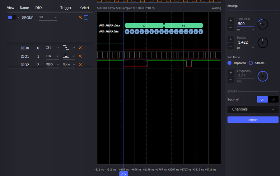
You can check the result using the formula for ADC transfer function, where the MISO data is the digital output code, voltage read on Oscilloscope Channel 1 is the analog input, voltage read on Oscilloscope Channel 2 is the reference input, and N is the number of bits of the AD7920.


From the above computation it results that the ADC input voltage is 1.5 V, the same value read on Oscilloscope Channel 1.
Extra Activity: Dual-Slope ADC
The dual-slope ADC (or a variant) is at the heart of many of the most accurate digital voltmeters. This architecture has a few useful characteristics: only a few precision components are required as most error sources cancel out, it can be configured to reject particular noise frequencies such as 50 Hz or 60 Hz line noise, and it is insensitive to high frequency noise.


The converter operates by applying the unknown input voltage to an integrator for a fixed time period (called runup), after which a known reference voltage, of opposite polarity to the input, is applied to the integrator (called rundown). Thus, the input voltage can be calculated from the reference voltage and the ratio of the rundown to runup times:


By inspection, the accuracy of the dual-slope converter is not affected by the tolerance of most of the components:
- The integrator’s resistor and capacitor tolerance will affect the slope of the output, but it will affect both runup and rundown equally.
- Errors in the time base used to set the runup time and measure the rundown time will affect both times equally.
The reference voltage does need to be accurate, as it directly affects the measurement. Another error source is dielectric absorption in the integrator capacitor, so polypropylene or polystyrene is ideal, and aluminum electrolytic are not appropriate.


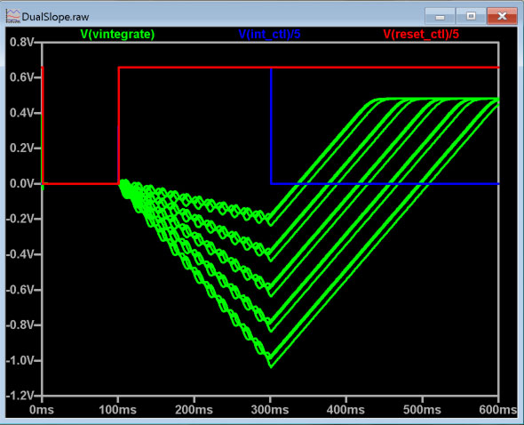
Figure 26 shows the frequency response of a dual-slope ADC. The input is sampled for a fixed time interval (runup)—the voltage at the beginning of runup has as much influence on the result as the voltage at the end of runup. This is sometimes called a boxcar average, and it has the effect of rejecting disturbances (noise) that occur at frequencies of 1/T, 2/T, 3/T, etc. An integration time of 200 ms corresponds to 10 cycles of 50 Hz noise, and 12 cycles of 60 Hz noise, so this is often chosen as the runup time as it rejects line noise in any country in the world.
Simulation
Open the LTspice® file DualSlope.asc available here.


Run the simulation, probing the Vintegrate node.

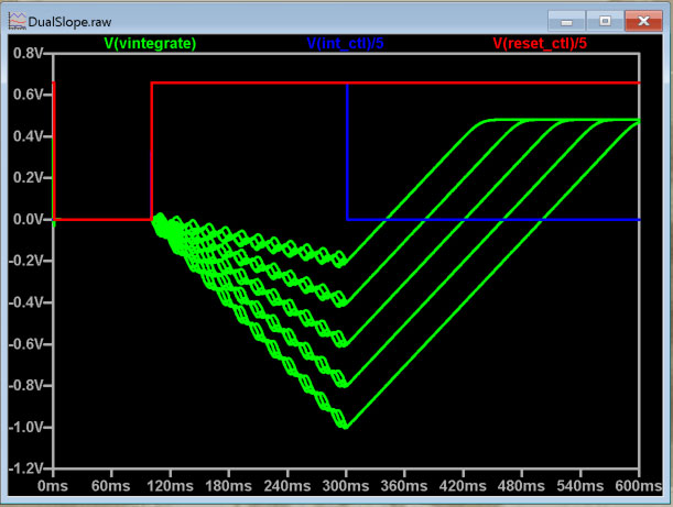
The simulation adds 60 Hz line noise to a DC input voltage. Several cases are run by the .step directive—input voltages of 1 V, 2 V, 3 V, 4 V, 5 V, and several different phases of the 60 Hz line noise. Because the 200 ms runup time is an integer number of 60 Hz line cycles, the noise falls into a null in the frequency response and rundown time is unaffected, regardless of phase. Change the frequency to 62.5 Hz, which lies at a peak in the frequency response.

Hardware Setup
Build the breadboard circuit for the dual-slope ADC as shown in Figure 30, and make the indicated connections to the M2K.


Procedure
Open Scopy. A Scopy initialization file, Dual_slope_scopy_setup.ini, is included to aid in setup.
Power Supply: Tracking enabled, set to ±5 V.
Digital IO: DIO2 set to OUT, set to 1.
Pattern Generator: Group DIO0, DIO1, Pattern: Import (load file dual_slope_pattern.csv). Frequency set to 5 Hz.
Signal Generator: Channel 1 initially set to constant 2.5 V.
Oscilloscope: 200 ms time base, Channel 1 set to 400 mV/division. Falling-edge trigger, 200 mV (this triggers the M2K at the start of the integrator’s reset interval).

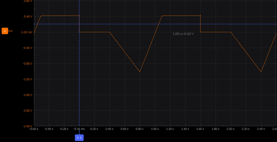
With the reference tied to the –5 V supply and the input voltage set to 2.5 V, notice that rundown is 2 divisions (400 ms) while runup is 1 division (200 ms). Thus:
VIN = 5 V × (200 ms / 400 ms) = 2.5 V
By varying the input voltage, we can notice a change in the runup time. A plot is presented in Figure 32.

A practical implementation of a dual-slope converter would use a microcontroller to control the integrator and set the runup/measure the rundown times. Most microcontrollers have counter peripherals, making this an easy task.
Question:
1. Can you name several real-world applications of ADCs?
You can find the answer at the StudentZone blog.


