Objective
The objective of this activity is to investigate the simple NPN emitter follower amplifier, also sometimes referred to as the common collector configuration.
Materials
- ADALM2000 Active Learning Module
- Solderless breadboard
- Jumper wires
- One 2.2 kΩ resistor (RL)
- One small signal NPN transistor (2N3904 for Q1)
Directions
The breadboard connections are shown in Figure 2. The output of the arbitrary waveform generator, W1, is connected to the base terminal of Q1. Scope Input 1+ (single ended) is also connected to the W1 output. The collector terminal is connected to the positive (Vp) supply. The emitter terminal is connected to both the 2.2 kΩ load resistor and Scope Input 2+ (single ended). The other end of the load resistor is connected to the negative (Vn) supply. To measure the input to output error, Channel 2 of the scope can be used differentially by connecting 2+ to the base of Q1 and 2– to the emitter.


Hardware Setup
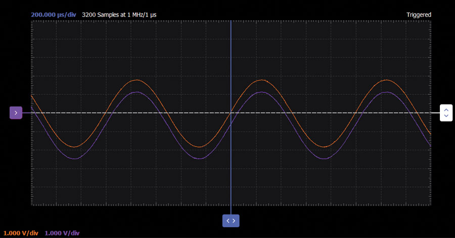
The waveform generator should be configured for a 1 kHz sine wave with 4 V amplitude peak-to-peak and 0 offset. The single-ended input of Scope Channel 2 (2+) is used to measure the voltage at the emitter. The scope configured with Channel 1+ is connected to display the AWG generator output. When measuring the input to output error, Channel 2 of the scope should be connected to display the 2+ and 2– differential.


Procedure
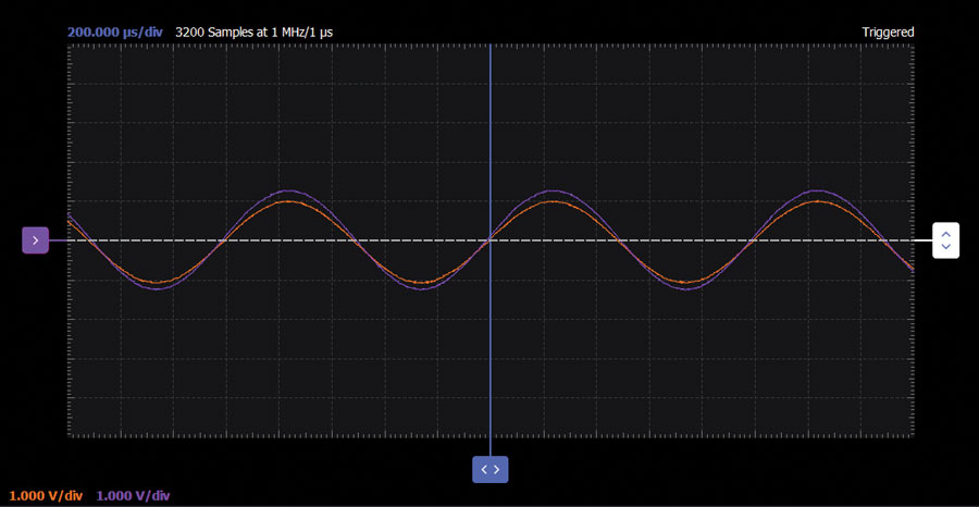
Configure the oscilloscope instrument to capture several periods of the two signals being measured. A plot example is presented in Figure 3.

The incremental gain (VOUT/VIN) of the emitter follower should ideally be 1 but will always be slightly less than 1. The gain is generally given by the following equation:

From the equation we can see that in order to obtain a gain close to 1 we can either increase RL or decrease re. We also know that re is a function of IE and that as IE increases, re decreases. Also, from the circuit we can see that IE is related to RL and that as RL increases, IE decreases. These two effects work counter to each other in the simple resistive loaded emitter follower. Thus, to optimize the gain of the follower we need to explore ways to either decrease re or increase RL without affecting the other. Looking at the follower in another way, because of the inherent DC shift due to the transistor’s VBE, the difference between input and output should be constant over the intended swing. Due to the simple resistive load, RL, the emitter current, IE, increases and decreases as the output swings up and down. We know that VBE is an exponential function of IE and will change approximately 18 mV (at room temperature) for a factor of 2 change in IE. In this +2 V to –2 V swing example, the minimum IE = 2 V/2.2 kΩ or 0.91 mA and the maximum IE = 6 V/2.2 kΩ or 2.7 mA. This results in a 28 mV change in VBE. This observation leads us to the first possible improvement in the emitter follower. To fix the amplifier transistor emitter current, the current mirror from the “ADALM2000 Activity: BJT Current Mirror” is now substituted for the emitter load resistor. A current mirror will sink a more or less constant current over a wide range of voltages. This more or less constant current flowing in the transistor will result in a fairly constant VBE. Viewed another way, the very high output resistance of the current source has effectively increased RL while re remains at a low value set by the current.
Improved Emitter Follower
Additional Materials
- One 3.2 kΩ resistor (use a 1 kΩ in series with a 2.2 kΩ)
- One small signal NPN transistor (2N3904 for Q1)
- Two small signal NPN transistors (SSM2212 for Q2 and Q3) selected for best VBE matching
Directions
The breadboard connections are shown in Figure 4 and Figure 5.


Hardware Setup
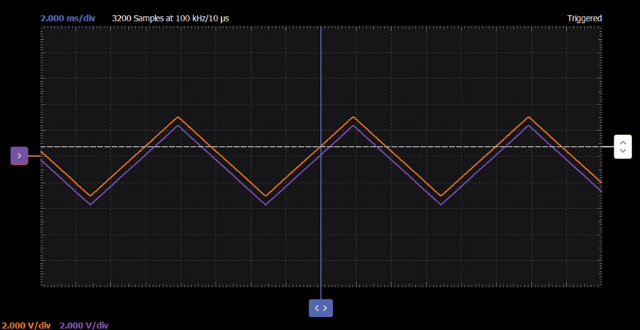
The waveform generator should be configured for a 100 Hz triangle wave with 3 V amplitude peak-to-peak and 0 offset. The single-ended input of Scope Channel 2 (2+) is used to measure the voltage at the emitter of Q1. The scope configured with Channel 1+ is connected to display the AWG generator output. When measuring the input to output error, Channel 2 of the scope should be connected to display the 2+ and 2– differential.


Procedure
Configure the oscilloscope instrument to capture several periods of the two signals being measured. A plot example is presented in Figure 6.


Low Offset Follower
The follower circuit we have investigated so far has a built-in offset of –VBE. The circuit shown next uses the VBE shift up of a PNP emitter follower to partially cancel the VBE shift down of an NPN emitter follower.
Materials
- One 6.8 kΩ resistor
- One 10 kΩ resistor
- One 0.01 μF capacitor
- One small signal PNP transistor (2N3906 for Q1)
- Three small signal NPN transistors (2N3904 or SSM2212 for Q2, Q3, and Q4)
Directions
The breadboard connections are shown in Figure 8 and Figure 9. The output of the function generator is connected to the base terminal of PNP transistor Q1. The collector terminal of Q1 is connected to diode connected NPN Q3, which is the input of a current mirror. The emitter terminal is connected to both resistor R1 and the base terminal of NPN transistor Q2. Scope Input 2+ is connected to both the emitter of Q2 and the collector of Q4. The emitters of both Q3 and Q4 are connected to the negative (Vn) supply. For best transistor matching, use the SSM2212 matched NPN pair for Q3 and Q4.


Hardware Setup
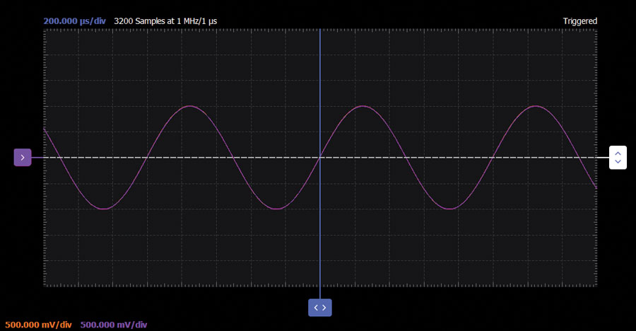
The waveform generator should be configured for a 1 kHz sine wave with 4 V amplitude peak-to-peak with the offset set equal to 0. Scope Input Channel 2 is set to 500 mV/div.


Procedure
Configure the oscilloscope instrument to capture several periods of the two signals being measured. A plot example is presented in Figure 10.

A problem can be identified when the simple emitter follower drives a capacitive load. The rise time of the output can be relatively fast as the emitter current is limited only by beta times the base current that can be supplied by the signal source driving the base. The fall time can be much slower and is limited by either the emitter resistor or current source.
Balanced Slew Rate Follower
Materials
- Two 2.2 kΩ resistors
- One 10 kΩ resistor
- One 0.01 μF capacitor
- Three small signal PNP transistors (2N3906 or SSM2220 for Q2, Q3, and Q4)
- Three small signal NPN transistors (2N3904 or SSM2212 for Q1, Q5, and Q6)
Directions
The circuit shown in Figure 11 uses feedback to adjust the current in the emitter follower as the current in the load changes. The current to pull the output negative can be as much as N (the gain of the NPN mirror) times the current in PNP Q3. For best transistor matching, use the SSM2220 matched PNP pair for Q3 and Q4 and the SSM2212 matched NPN pair for Q5 and Q6 (NPN mirror gain will be 1. Add a second SSM2212 in parallel with Q5 to increase the mirror gain).


Hardware Setup
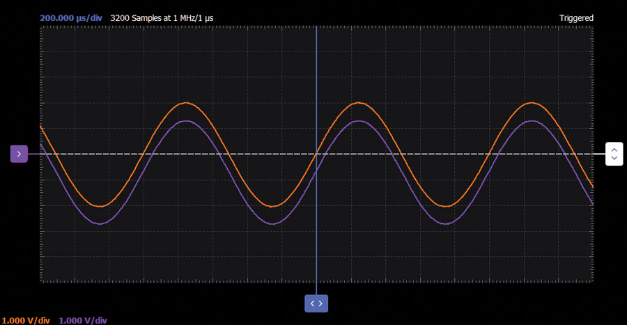
The waveform generator should be configured for a 1 kHz sine wave with 4 V amplitude peak-to-peak with the offset set equal to 0. Scope Input Channel 2 is set to 1 V/div.


Procedure
Configure the oscilloscope instrument to capture several periods of the two signals being measured. A plot example is presented in Figure 13.

An alternate approach to improving the emitter follower is to reduce the effective re through negative feedback. Reducing re can be addressed by adding a second transistor to increase the negative feedback factor by increasing the open-loop gain. The single transistor is replaced by a pair with 100% voltage feedback to the emitter of the first transistor. This is often referred to as a complementary feedback pair. The value of R2 is crucial to good linearity, as it sets the IC of transistor Q1, and also determines its collector loading.
Complementary Feedback Pair Emitter Follower
Materials
- One 2.2 kΩ resistor
- One 10 kΩ resistor
- One small signal NPN transistor (2N3904 for Q1)
- One small signal PNP transistor (2N3906 for Q2)
Directions
The breadboard connections are shown in Figure 14 and Figure 15.


Hardware Setup
The waveform generator should be configured for a 1 kHz sine wave with 2 V amplitude peak-to-peak with the offset set equal to 0. Scope Input Channel 2 is set to 1 V/div.


Procedure
Configure the oscilloscope instrument to capture several periods of the two signals being measured. A plot example is presented in Figure 16.

Question:
Can you name three specific characteristics of the emitter follower circuits? You can find the answer at the StudentZone blog.

