QUESTION:
If I am trying to improve the efficiency of my system or reduce component count, can I tweak my RSENSE value or remove the RSENSE filtering components?

Answer:
Choosing an RSENSE value that is too large or too small, as well as removing the filtering, can lead to worse system efficiency and degraded noise performance.
Abstract
This is the second article in a series where common switch-mode power supply (SMPS) design errors will be discussed as well as their appropriate rectification. This article aims to address complications that arise with the feedback stage design of DC-to-DC switching regulators, focusing on the sense resistor (RSENSE) component. RSENSE is critical to ensuring the feedback network (which is responsible for maintaining the output voltage) receives an accurate signal from the inductor current. A distorted signal can make the inductor ripple appear larger or smaller than it actually is, resulting in the feedback network behaving in unintended ways.
Introduction
In this article, buck converters are used to demonstrate the effects of incorrectly sizing the sense resistor, as well as what happens when the RSENSE filter components are removed. A detailed introduction to the operation of buck converters can be found in the first article of this series, “Analysis of Switch-Mode Power Supply Inductor Design Violations and Rectification.” The sense resistor is often incorrectly sized because designers attempt to optimize efficiency and operation, but incorrect sizing leads to degraded performance. In addition, the sense resistor filter components are critical to provide accurate information to the feedback architecture, and, when removed, can worsen the SMPS performance.
What Is the Sense Resistor?
The current coming out of the inductor is converted into a voltage via a small sense resistor (RSENSE). This can be seen in Figure 1.
|
Figure 1. A simplified schematic demonstrating the basic operation of buck converters and their feedback system. This diagram can be found in application note AN-140. |

This voltage acts as the signal sent to the feedback logic to regulate the output. Choosing the correct value for this sense resistor is critical to ensure that the feedback logic is receiving an accurate depiction of the inductor current. Furthermore, it ensures that the RSENSE signal conforms to the data sheet’s absolute maximum differential voltage across the sense resistor.
Complications of an Undersized Sense Resistor
Designers may choose to decrease the value of their sense resistor in order to achieve better efficiency. The sense resistor is included in series with the inductor and the output so that the device can sense the triangular inductor current waveform and use it in the feedback loop. Power losses in this resistor are determined by Ploss = I2L × RSENSE. By decreasing the value of the sense resistor, the designer can slightly improve their efficiency. However, this comes at a cost. If the resistor is too small, the signal from the sense resistor will be too small as well. This leads to a worse signal-to-noise ratio (SNR), as noise becomes close in magnitude to the converted signal from the inductor current. With a weaker SNR, the sense resistor can no longer isolate the primary signal, leading to noise riding on the output signal. This is usually observed as jitter on the output signal, which can be seen in Figure 2.
|
Figure 2. Jitter caused by the instability in the output. The waveform shown with the persist feature is the undersized RSENSE output waveform. The highlighted waveform is captured with the nominal RSENSE. |

To fix this, designers should choose a proper RSENSE value according to this formula:

Where Vsense(max) is determined in the device’s data sheet, and Imax is the maximum load current that one will draw. Each SMPS can handle a maximum current (Imax) that is defined as the sum of half the inductor current ripple and the average load current, which is visualized in Figure 3.

|
Figure 3. Inductor current waveform. |

Choosing the value according to this formula ensures that the RSENSE value is large enough to adequately capture the inductor current ripple. If designers are having trouble choosing the proper value, they can utilize Analog Devices’ LTpowerCAD®, which will calculate and provide a suggested RSENSE value to ensure proper operation. If designers are concerned with the efficiency of their design, they can also utilize the Power Loss and Efficiency tab in LTpowerCAD to determine sources of power loss in the circuit, such as MOSFET switching losses and inductor DCR losses, and rectify those by choosing more efficient components. Additionally, if a part has inductor DCR sensing capabilities, the sense resistor can be omitted, and the voltage sensing occurs across the inductor in order to increase efficiency at the cost of reliability and noise performance. Using the sense resistor is the preferred method, but inductor DCR sensing of the current waveform can be done if peak efficiency is necessary.
Complications of an Oversized Sense Resistor
Designers typically will not choose an oversized sense resistor when designing their SMPS. However, issues with layout can lead to the resistance of PCB traces adding to the value of the sense resistor and increasing the total sense resistance. Typically, SMPS chips have a current limiting feature that is determined by a maximum voltage that can be developed across the sense resistor. When this value is exceeded, the part goes into a current limiting mode, and the output voltage begins to droop as the load current increases. The part no longer regulates the output voltage. This can be seen in Figure 4.
|
Figure 4. Load regulation for an oversized sense resistor. This specific DC-to-DC converter is rated up to 15 A but stops regulating at around 4 A with an oversized sense resistor. |

This phenomenon often occurs when the traces between the inductor and the sense resistor are longer than they need to be, or when the current-carrying trace is connected to one of the sense pins on the chip. Since the chosen sense resistor is in the milliohm range, it is sensitive to any added resistance. Preventing this issue can be achieved by a Kelvin connection, which is demonstrated in Figure 5.
|
Figure 5. This is an example of a proper Kelvin connection. |

The sense traces come from the sense resistor and are separate from the PCB pad and the current-carrying traces. The Kelvin traces are much thinner and are as close to the sense resistor as possible to avoid added parasitic resistance. This allows VSENSE to be an accurate representation of just the voltage across the sense resistor. Therefore, when the sense resistor increases due to a lack of proper Kelvin connections, long traces, or simply choosing the wrong value, the current limit is tripped at lower loads because the VSENSE(MAX) is reached much sooner, leading to worse load regulation.
What Is Equivalent Series Inductance (ESL)?
Due to the low value of the sense resistor (which is in the milliohm range), the parasitic equivalent series inductance (ESL), an inherent characteristic of surface mount device (SMD) resistors, has a noticeable effect on the sensing architecture. As such, an RC filter must be added to the sense traces to negate the effect of the parasitic ESL. Designers do not have a perceived advantage to leaving out these components but may do so to reduce BOM size and cost or may simply forget to include these components.
ESL is not only made of the sense resistor parasitic inductance, but also general inductance caused by board layout and wire tracing. ESL can be calculated with Equation 3:

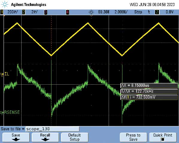
VESL(step) is the added voltage across the sense resistor. The filter needs to yield an RC time constant that is equal to or smaller than the calculated sense resistor time constant (ESL/R). When this filter is removed, the sense resistor will exhibit inductive characteristics superimposed on its resistive characteristics. These can be observed by the spikes (voltage step) on the sense resistor waveform, as seen in Figure 6.
|
Figure 6. This is the RSENSE signal when the filter compensation system is removed. |
Furthermore, due to the increased output ripple, the device wrongfully assumes it has reached its internal current limit at a lower load rating, resulting in worse load regulation.
|
Figure 7. Load regulation of the power supply when the filter compensation system is removed. This specific device is rated up to 15 A but stops regulating at 12 A. |

This issue can be fixed by adding a properly sized filter. This filter can be determined by the formula shown in Figure 8.
|
Figure 8. Suggested filter compensation RC specifications. Obtained from LTC3855 data sheet. |

After doing so, the voltage delivered to the sense architecture will improve. Compared to the signal across the sense resistor without the filter, it is clear that the RC filter smooths out the signal and eliminates the ESL step. The inductive spikes vanish and the waveform will look triangular, as expected. This can be seen in Figure 9.
|
Figure 9. This is the RSENSE signal when the filter compensation system is in place. The signal is measured across the filter capacitor because that is the output of the filter and what is going into the feedback system. |

Conclusion
This article serves as a guideline to analyze sense resistor design issues in the case of buck converters. Furthermore, it provides practical solutions in case designers see any of the unwanted performance depicted in this article. Although often overlooked, the sizing of the sense resistor is essential to maintaining a stable output voltage with varying loads. Choosing an improperly sized sense resistor to save power, or not accounting for layout resistor parasitics, can lead to degraded performance of the system as a whole. Additionally, neglecting the sense resistor filtering components will result in an inaccurate signal fed back to the sensing architecture and will further degrade the system’s performance.
Part 1: Analysis of Switch-Mode Power Supply and Rectification: Inductor Violations
Part 3: Analysis of Switch-Mode Power Supply and Rectification: Transistor Timing & Boost Capacitor Issues


