Abstract
In most lab environments, signal generators, spectrum analyzers, etc., are single-ended instruments used to measure the distortion of high speed differential amplifier drivers and converters. As a result, measuring even order distortion on the amplifier driver, such as second-harmonic distortion, HD2, and even order intermodulation distortion or IMD2, requires additional components like baluns and attenuators as part of the overall test setup to interface single-ended test instrumentation to the differential inputs and outputs of the amplifier driver. This article reveals the importance of phase imbalance going through the math of mismatched signals and how phase imbalance leads to an increase (meaning worse!) in even order products. It will also demonstrate how the use of trade-offs of several different high performance baluns and attenuators can affect these performance metrics (that is, HD2 and IMD2) of the amplifier under test.
Math Background = Yay!
Magnitude and phase imbalance are important specifications to understand when testing high speed devices that have differential inputs, such as analog-to-digital converters, amplifiers, mixers, baluns, etc.
Great care must be taken when implementing analog signal chain designs that use 500 MHz frequencies and above as all devices, active or passive, have some sort of inherent imbalance across frequency. Not that 500 MHz is by any means a magic frequency point, it is just that, based on experience, this is where most devices start to deviate in phase balance. Depending on the device, this frequency could be much lower or higher.
Let’s take a closer look in detail using this simple mathematical model below:
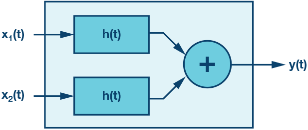
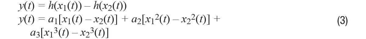
Consider the inputs x(t) to an ADC, amplifier, balun, etc., or any device that converts signals from single-ended to differential, or vice versa. The pair of signals, x1(t) and x2(t), are sinusoidal and, therefore, the differential input signals are of the form below:

If not, even order distortion test results of the ADC can dramatically vary over the operating frequency range directly due to the amount of imbalance in these components.
The ADC, or any active device for that matter, can be simply modeled as a symmetrical third-order transfer function:

Then,
In the ideal case, where we have no imbalance, the transfer function of the simple system above can be modeled as follows:
When x1(t) and x2(t) are perfectly balanced, they have the same magnitude (k1= k2= k) and are exactly 180o out of phase (φ = 0°).


When applying the trigonometric identity for powers and gathering terms of like frequency we get:

This is the familiar result for a differential circuit: even harmonics cancel for ideal signals, while odd harmonics do not.
Now suppose the two input signals have a magnitude imbalance, but no phase imbalance. In this case, k1≠ k2, and φ = 0.

When we substitute Equation 7 for Equation 3 and again apply the trigonometric power identities—I know, ouch!
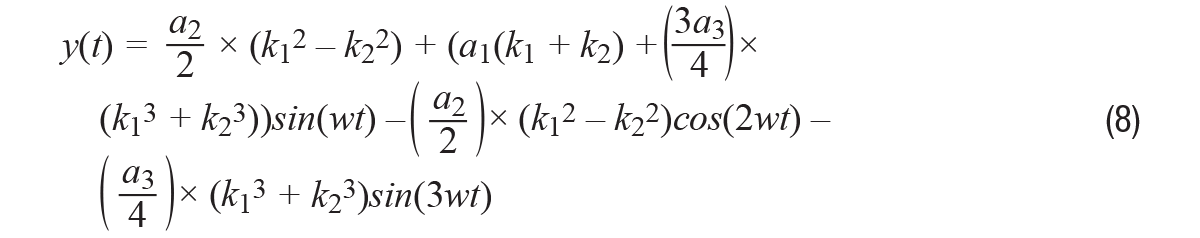
We can see from Equation 8 that the second harmonic is proportional to the difference of the squares of the magnitude terms k1 and k2, or simply put:

Now, let’s assume that the two input signals have a phase imbalance between them with no magnitude imbalance. Then, k1 = k2, and φ ≠ 0.

Substitute Equation 10 in Equation 3 and simplify—push through, you can do it!
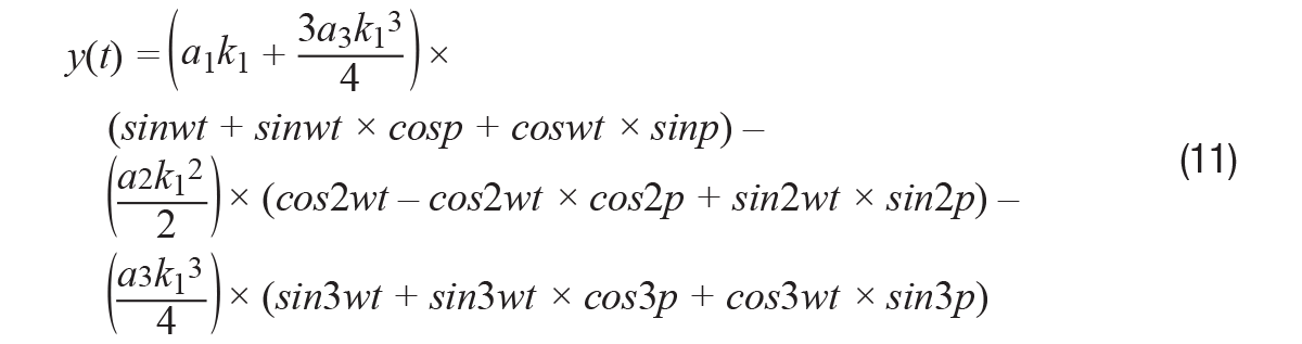
From Equation 11, we see that the second-harmonic amplitude is proportional to the square of the magnitude term, k.

If we go back and do a comparison of Equation 9 and Equation 12, and we assume my trigonometry IDs are in good shape, it all boils down to this; the second harmonic is more severely affected by phase imbalance than by magnitude imbalance. Here is why: for phase imbalance, the second harmonic is proportional to the square of k1—again, look at Equation 12, while for magnitude imbalance, the second harmonic is proportional to the difference of the squares of k1 and k2, or Equation 9. Since k1 and k2 are approximately equal, this difference typically ends up being small—especially if you compare it to a number that is squared!
Testing HS Amplifiers
Now that we cleared that hump, let’s move onto a use case, as is shown in Figure 2. Here, we see a block diagram that shows a test setup for HD2 distortion testing typically used in the lab of a differential amplifier.
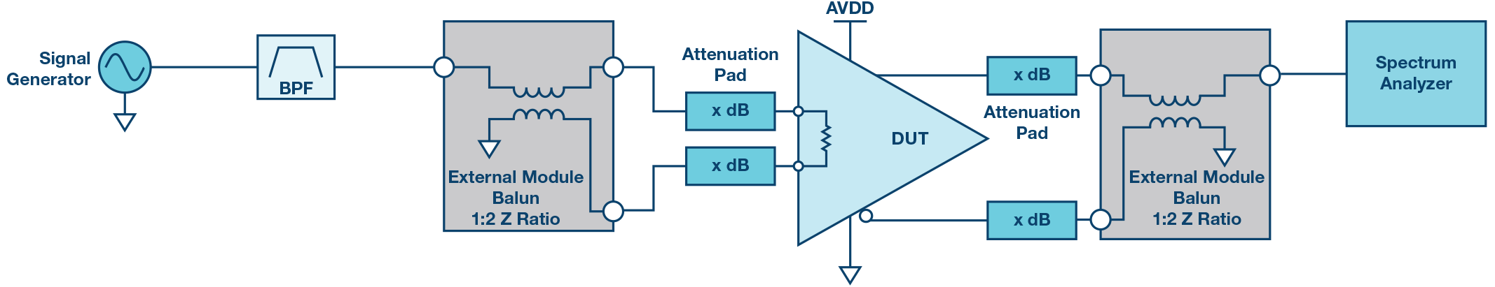
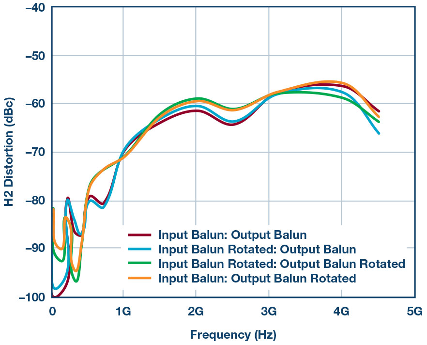
At first glance, this seems pretty straightforward—however, the devil is in the details of this test. If we look at Figure 3, we see a battery of HD2 test results using all the same components in this block diagram, differential amplifier, baluns, attenuators, etc. What was completed in these tests was to show that the simple mismatch in phase, just by flipping the balun orientation in different ways, can produce different results across the HD2 frequency sweep. There are two baluns in this setup, so this can create four possible scenarios by reversing their connections on one or both sides of the setup. The results are shown in Figure 3.
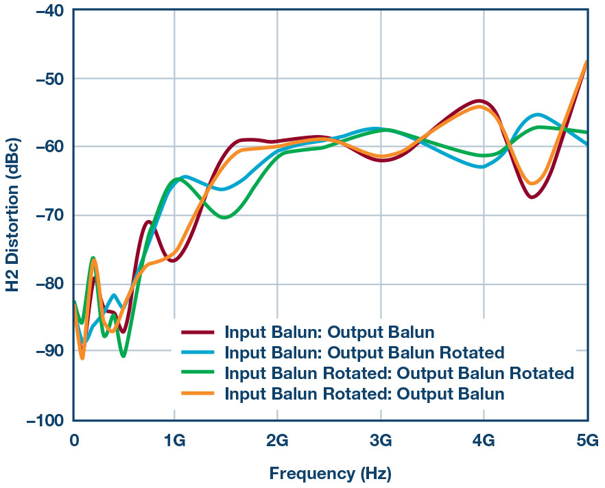
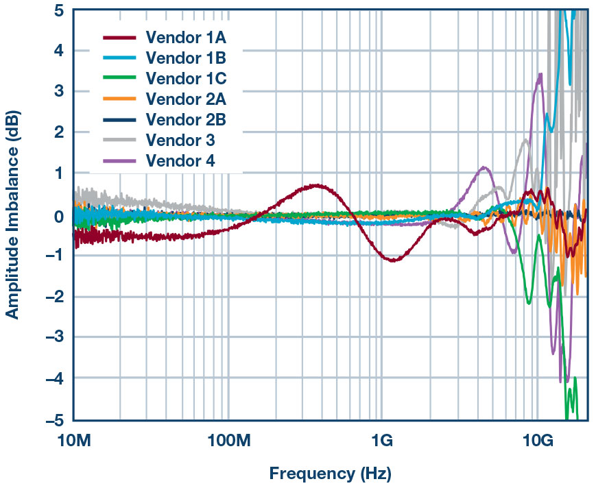
The amount of variance in HD2 distortion curves revealed in Figure 3 proves a further look at the balun’s performance is needed, specifically for phase and magnitude imbalance. The following two figures show the phase and magnitude imbalance of several baluns from various manufacturers. A network analyzer was used for the imbalance test measurements.
The red traces in Figures 4 and Figure 5 correspond to the actual balun used to acquire HD2 distortion data in Figure 3. This particular balun, from Vendor 1A, had one of the highest bandwidths and good pass-band flatness, but worse phase imbalance as compared to the other baluns over the same 10 GHz frequency test band.
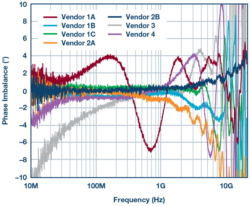
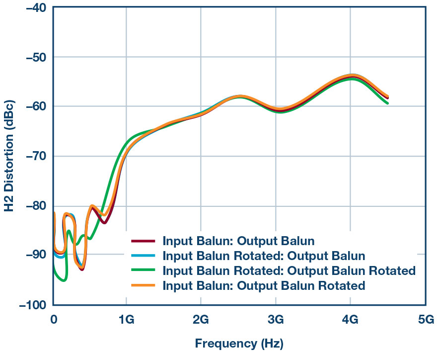
The next two figures represent a retest of HD2 distortion using the best balun that had the lowest phase imbalance found in Figure 6 and Figure 7, from Vendor 1B and Vendor 2B, respectively. Notice that with better imbalance performance, HD2 distortion variance is reduced accordingly, as seen in Figure 7.
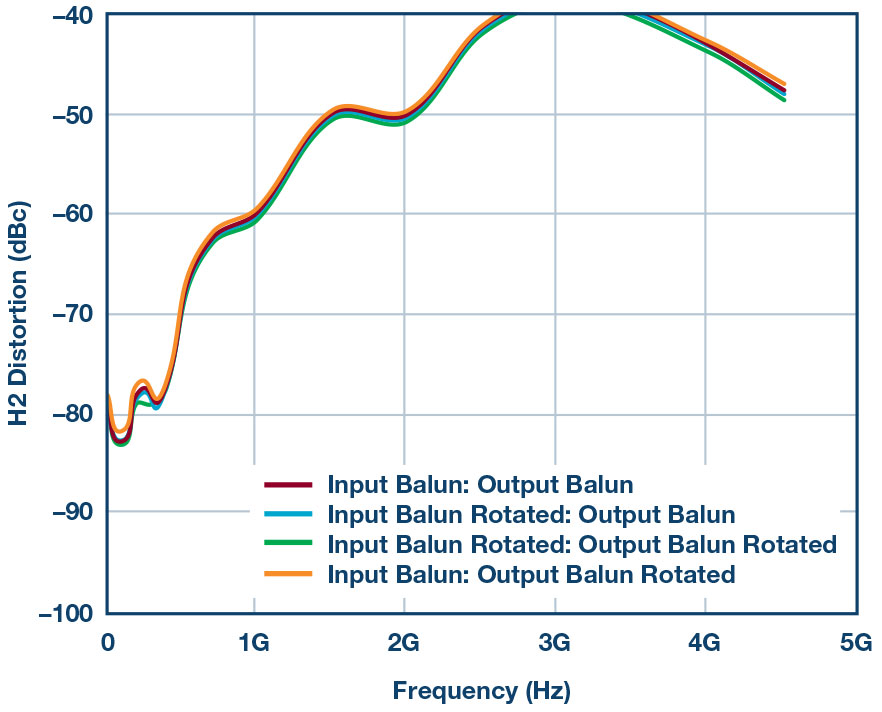
To further illustrate how phase imbalances directly affects the performance of even order distortion, Figure 8 shows HD3 distortion over the same conditions as the previous HD2 figure. Notice how all four traces are roughly the same, as expected. Therefore, as proven in the mathematical derivation example shown previously, HD3 distortion is not as sensitive to imbalances in the signal chain.
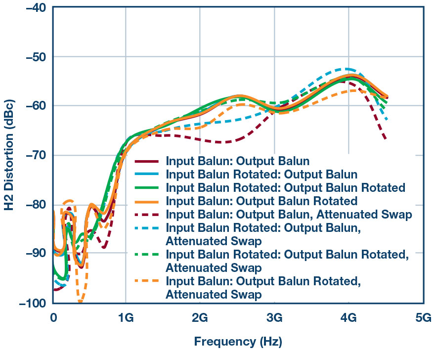
Until this point it should be assumed that the input and output connected attenuator pads, as shown connected in Figure 2, are stationary and did not change during the balun orientation measurements. The next figure represents the same traces shown in Figure 7, testing only Vendor 2B’s balun performance as the attenuators are swapped between the inputs and outputs. This generates another set of four traces, shown as dashed lines in Figure 9. The result is that we are back where we started, as this shows up as more variation in the test measurement. This further underscores that small amounts of mismatch in either side of a differential signal pair matters at high frequencies. Keep in mind to document your test conditions in detail.
Balancing It All Out
In summary, all things matter when developing fully differential signal chains in the GHz regions; that is, attenuators pads, baluns, cables, traces on a PC board, etc. We have proven this mathematically and in the lab using a high speed differential amplifier as our test bed. So, before we start to blame the part or the vendor, please take extra special care during the PCB layout and lab testing.
Lastly, you might be asking yourself, so how much phase imbalance can I tolerate? When I pick up a balun, for example, and it says x number of degrees of phase imbalance at x GHz, what does that mean in terms of degradation to my part or system? Can I expect a certain amount of loss or degradation in dB’s of linearity performance?
This is a difficult question to answer. In the ideal world, if everything in your signal chain were matched perfectly, there would be no even order distortion to contend with. Second, it would be nice to have a rule of thumb or equation that says for every x° of phase imbalance, one should expect x dBs of loss in linearity (HD2 degradation). However, this just cannot be. Why? Because every component, be it active or passive and differential in nature, has some sort of inherent phase mismatch. There is just no way to perfectly balance an IC design internally, or cut cables with absolute perfectly matched length. So, no matter how small these mismatches are, they become more pronounced as higher and higher frequencies are utilized in a system.
Let’s wrap this up by saying we will do our job as best we can by keeping those IC layout mismatches small where fully differential inputs and outputs are used. We hope you do the same when testing our products in the lab.

