The Fundamentals of LDO
The Fundamentals of LDO Design and Applications
- ADIsimPower Design Tool (Web)
- ADI Linear Regulator Design Tool and Parametric Search (Download)
- The Fundamentals of LDO Design and Application (pdf)
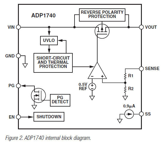
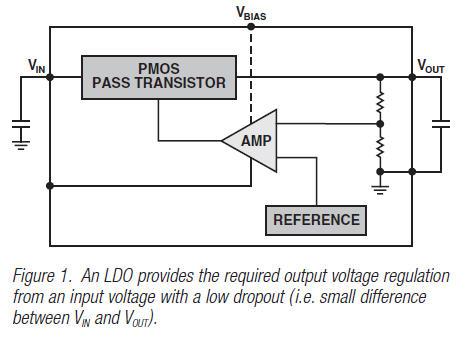
A low dropout regulator (LDO) consists of a voltage reference, an error amplifier, a feedback voltage divider, and a series pass element, usually a bipolar or CMOS transistor (see Figure 1). Output current is controlled by the PMOS transistor, which in turn is controlled by the error amplifier. This amplifier compares the reference voltage with the feedback voltage from the output and amplifies the difference. If the feedback voltage is lower than the reference voltage, the gate of the PMOS device is pulled lower, allowing more current to pass and increasing the output voltage. If the feedback voltage is higher than the reference voltage, the gate of the PMOS device is pulled higher, allowing less current to pass and decreasing the output voltage. This is a closed-loop system based around two main poles, the internal pole of the error amplifier/pass transistor and the external pole of the output capacitor’s equivalent series resistance (ESR).
Analog Devices LDOs are designed to be stable over the specified operating temperature and voltage ranges when the recommended capacitors are used. The ESR of the output capacitor affects the stability of the LDO control loop. A minimum ESR of 1 Ω or less is recommended to ensure stability. The LDOs response to rapid changes in load current, i.e. the transient response, is also affected by output capacitance. Using a larger value of output capacitor improves the transient response of the LDO; however, it can increase the start-up time.
LDO regulators are used to derive lower output voltages from a main supply or battery. The output voltage is ideally stable with line and load variations, immune to changes in ambient temperature, and stable over time. LDOs should have as low a difference between the input and output voltage as possible, called the dropout voltage. For example, in a battery-powered design using a lithium-ion cell connected to a 2.8 V LDO, the battery voltage can drop from 4.2 V (fully charged) to 3.0 V (battery empty) and provide a constant 2.8 V output provided the LDO’s dropout voltage is below 200 mV. In some systems LDOs are used for postregulation. The LDO connects to the output of a high-efficiency switching regulator and provides noise filtering, as well as a constant and stable output voltage.
Depending on your particular design your selection criteria may differ. However, as a general rule you should use the list below in the order that they appear.
- Input voltage range
- Output voltage, fixed or adjustable
- Output accuracy over line, load, and temperature
- Load current requirement
- Dropout voltage
- Power supply rejection ratio (PSRR)
- Output noise
- Quiescent current and shutdown current
An LDO’s design is usually optimized for a specific value of load bypass capacitor. Increasing the load capacitance above the recommended value can improve load transient response. However, when a larger output capacitor is chosen, the input bypass capacitor should be increased to match it. Note: the input and output capacitors should be placed as close as possible to the LDO.
Any good quality ceramic capacitors can be used, as long as they meet the minimum capacitance and maximum effective series resistance (ESR) specifications listed on the LDO data sheet. Ceramic capacitors using X5R or X7R dielectrics are highly recommended as these have good temperature stability and a low voltage coefficient.
Designs using a bipolar transistor for the pass element exhibit a large increase in ground current as output load increases, reaching ~5% of load current. MOSFET based LDOs are more energy efficient as the ground current increase with load is minimal. The ground current for MOSFET based LDOs is typically below 0.1% of full load.
Power supply rejection ratio specifies the ability of an LDO to prevent output voltage fluctuations when there are variations in input voltage. PSRR is usually specified at a specific frequency, for example 60 dB rejection at 120 Hz. Battery-based systems should employ LDOs that maintain high PSRR at low battery voltages, i.e. with a low input-output voltage differential.
LDOs will reject input noise up to tens, even hundreds of kHz. High frequency (1 MHz and up) switching noise rejection is primarily a function of the output bypass capacitor network; the LDO’s loop bandwidth is too low above 1 MHz to provide any noise reduction. The LDO forms an impedance divider with the pass element and the output capacitor network and load; this provides noise rejection at high frequency.
An LDO’s internal voltage reference is the primary source for output noise. It is usually specified in microvolts rms over a specific bandwidth, such as 25 ìV rms from 1 kHz to 100 kHz. This low level noise is much lower than the switching transients and harmonics from a switch mode dc-to-dc converter. Some LDOs feature a bypass pin to filter reference voltage noise with a capacitor to ground. Following the data sheet specified input, output, and bypass capacitors usually results in a unproblematic noise level.
None of Analog Devices LDOs need a minimum load current. However, there are many competitive LDOs on the market that do require a minimum load, some needing as much as several mA.
- An enable input to control LDO turn-on and turn-off for system power savings
- Programmable soft-start to limit inrush current, control output voltage rise-time during startup, and enable voltage sequencing
- Tracking feature, which allows the LDO output to follow an external voltage rail or reference
- A bypass pin that allows an external capacitor to reduce output voltage noise and improve power supply rejection
- A power-good output that indicates when the output is in regulation
- Thermal shutdown that turns the LDO off if its temperature exceeds the specified level
- Current limit function to control the LDO’s output current and power dissipation