Objective
The objective of this activity is to investigate the simple differential amplifier using enhancement mode NMOS transistors.
The notes on hardware limitation issues presented in the June 2021 StudentZone article are valid also for this activity. The signal-to-noise ratio can be improved by increasing the signal level and then placing an attenuator and filter (see Figure 1) between the generator outputs and the circuit inputs. The materials needed for this activity are:
- Two 100 Ω resistors
- Two 1 kΩ resistors
- Two 0.1 μF capacitors (marked 104)


This attenuator and filter will be used in all parts of this lab.
Materials
- ADALM2000 Active Learning Module
- Solderless breadboard
- Jumper wires
- Two 10 kΩ resistors
- One 15 kΩ resistor (use a 10 kΩ in series with a 4.7 kΩ)
- Two small signal NMOS transistors (CD4007 or ZVN2110A)
Directions
The connections to the lab hardware are as indicated in Figure 2. M1 and M2 should be selected from the available devices with the best matching of Vth. The sources of M1 and M2 share a common connection with one end of R3. The other end of R3 is connected to the Vn (–5 V) and supplies the tail current. The gate of M1 is connected to the output of the first arbitrary waveform generator, and the gate of M2 is connected to the output of the second arbitrary waveform generator. The two drain load resistors R1 and R2 connect between the drains respectively of M1 and M2 and the positive supply Vp (+5 V). The differential scope inputs 2+/2– are used to measure the differential output as seen across the two 10 kΩ load resistors.


Hardware Setup
The first waveform generator should be configured for a 200 Hz triangle wave with 4 V amplitude peak-to-peak and 0 V offset. The second generator should also be configured for a 200 Hz triangle wave with 4 V amplitude peak-to-peak and 0 V offset but with 180° phase. Channel 1 of the oscilloscope should be connected with 1+ to the output of the first generator, W1, and 1– connected to W2. Channel 2 should be connected to display 2+ and 2– and set to 1 V per division.
Procedure
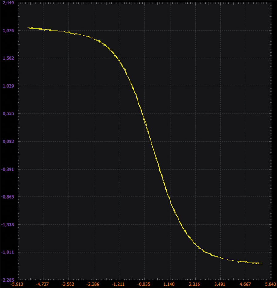
The following data should be taken: the x-axis is the output of the arbitrary waveform generator, and the y-axis is Scope Channel 2 using both the 2+ and 2– inputs. By changing the value of R3, the student can explore the effects of the level of the tail current on the gain of the circuit (as seen in the slope of the line as it passed through the origin) and the linear input range and the shape of the nonlinear curve fall off in the gain as the circuit saturates.

Using a Current Source as the Tail Current
The use of a simple resistor as the tail current has limitations. The student should explore ways to construct a current source to bias the differential pair. These could be made with a couple of additional transistors and resistors as in the stabilized current source from previous ADALM2000 activities.
Additional Materials
- Two small signal NMOS transistors (CD4007 or ZVN2110A for M3 and M4)


Hardware Setup
The first waveform generator should be configured for a 200 Hz triangle wave with 4 V amplitude peak-to-peak and 0 V offset. The second generator should also be configured for a 200 Hz triangle wave with 4 V amplitude peak-to-peak and 0 V offset but with 180° phase. The resistor dividers will reduce the signal amplitude seen at the gates of M1 and M2 to slightly less than 200 mV. Channel 1 of the oscilloscope should be connected with 1+ to the output of the first generator, W1, and 1– connected to W2. Channel 2 should be connected to display 2+ and 2– and set to 1 V per division.


Procedure
Configure the oscilloscope instrument to capture several periods of the two signals being measured. An XY plot example is presented in Figure 7.


Measuring Common-Mode Gain
Common-mode rejection (CMR) is a key aspect of the differential amplifier. CMR can be measured by connecting the gate of both transistors M1 and M2 to the same input source. Figure 10 shows the differential output for both the resistively biased and current source biased differential pair as the common-mode voltage from W1 is swept from +3 V to –3 V around ground. The gain will be affected the most as the transistors go from the saturation region to the triode (resistive) region as the positive voltage on the gates approaches the drain voltage. This can be monitored by observing the drain voltage single ended with respect to ground (that is, with the 2– input grounded). The amplitude of the generator should be adjusted until the signal seen at the output just starts to clip/fold over.


Hardware Setup
The waveform generator should be configured for a 100 Hz sine wave with 6 V amplitude peak-to-peak and 0 V offset. Channel 1 of the oscilloscope should be connected with 1+ to the output of the first generator, W1, and 1– to the ground. Channel 2 should be connected to display 2+ and 2– and set to 1 V per division.


Procedure
Configure the oscilloscope instrument to capture several periods of the two signals being measured. A plot example using LTspice® is presented in Figure 10.


Questions:
- Would you characterize the transistor amplifier in Figure 8 as being inverting or noninverting to outputs 2+ and 2– with the gate terminal of transistor M1 being considered the input? Explain your answer.
- Describe what happens to each of the output voltages (2+ and 2–) as the input voltage (W1) increases or decreases.
You can find the answers at the StudentZone blog.

