CN0506


Overview
Design Resources
Design & Integration File
- Schematic
- Bill of Materials
- Gerber Files
- Allegro Layout Files
- Assembly Drawing
Evaluation Hardware
Part Numbers with "Z" indicate RoHS Compliance. Boards checked are needed to evaluate this circuit.
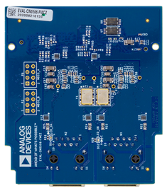
- EVAL-CN0506-FMCZ ($176.55) Dual Ethernet PHY Board
Device Drivers
Software such as C code and/or FPGA code, used to communicate with component's digital interface.
FPGA/HDL
Features & Benefits
- Supports RGMII, RMII, and MII modes
- Dual ports allow for ring or line topologies
- Can drive 154m of cable at 1000Mbsps
Product Categories
Markets and Technologies
Parts Used
Documentation & Resources
-
CN0506 User Guide10/5/2020WIKI
-
Solutions For Rapid Prototyping: Answering the Needs of Practicing Engineers8/23/2023PDF784 K
Circuit Function & Benefits
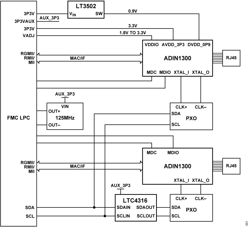
The circuit shown in Figure 1 is a dual channel, low latency, low power Ethernet physical layer (PHY) card that supports 10 Mbps, 100 Mbps, and 1000 Mbps speeds for industrial Ethernet applications using line and ring network topologies.
Dual channels enable line and ring network topologies that are commonly used for industrial sensing, control, and distributed control systems. The Ethernet PHY was extensively tested for electromagnetic compatibility (EMC) and electrostatic discharge (ESD) robustness and supports automatic negotiation to enable linking with remote PHY devices at the highest common speed advertised. IEEE 1588 time stamping in the PHY reduces timing uncertainty in real-time applications and enhances link loss detection for redundant and real-time applications.
The circuit consists of two individual, independent 10 Mbps, 100 Mbps, and 1000 Mbps PHYs, each with an energy efficient Ethernet (EEE) PHY core with all the associated common analog circuitry, input and output clock buffering, management interface, subsystem registers, media access control (MAC) interface, and control logic.
The design is powered from the host field programmable gate array (FPGA) mezzanine card (FMC) development board, eliminating the need for an external power supply. A software programmable clock enables media independent interface (MII), reduced MII (RMII), and reduced Gigabit MII (RGMII) MAC interface modes. RJ45 ports with integrated magnetics keep the solution as compact as possible. The solution supports cable lengths up to 150 meters at gigabit speeds and up to 180 meters at 100 Mbps or 10 Mbps.
This solution is typically used in ring or bus topologies. The automatic negotiation feature allows connection with other PHY devices at the highest supported speed.

Circuit Description
Ethernet
Ethernet is the most common type of packet-based physical connection for data networking applications in a local area network (LAN) that is defined as subsections and specifications by the Institute of Electrical and Electronic Engineers (IEEE) 802.3 standards.
There are different speeds and transmission medium associated with Ethernet. However, the focus of this circuit note centers on 10BASE-T, 100BASE-TX, and 1000BASE-T over twisted pair cables, Category 5e (CAT5e) or Category 6 (CAT6), straight through or crossover.
Line and Ring Network Topologies
Typical industrial Ethernet networks are deployed in line or ring topologies. The line and ring network topologies have reduced wiring lengths compared to start networks, and a redundant path for the ring network (see Figure 2). Each device connected to a line or ring network requires two Ethernet ports to pass Ethernet frames along the network.


PHY
A PHY is the physical interface transceiver that implements the physical layer functions of the open systems interconnection (OSI) model. A PHY encodes and decodes the data transmitted and received between devices, maintaining the integrity of the frames and packets (see Figure 3).

Figure 3. Typical Networked Sensor with PHY Device
PHY Hardware Configuration—Strapping Resistors
The ADIN1300 can be configured to power up ready to establish a link. This PHY hardware configuration uses external strapping resistors and provides a known configuration for power on in an unmanaged application. Typically, in unmanaged applications, users do not configure the PHY over the management data input and output (MDIO). Instead, unmanaged applications rely on the PHY hardware configuration to bring the ADIN1300 up with the appropriate configuration ready to link with a remote PHY partner. When the ADIN1300 powers up, the hardware strapping pins are sampled when the device comes out of reset, and the PHY device then knows how to configure the various functions.
The hardware configuration modes of interest for this circuit note are speed, PHY address, automatic medium dependent interface crossover (Auto-MDIX), and MAC interface. The EVAL-CN0506-FMCZ includes resistor footprints for the various combinations, with a particular default configuration. The resistor components can be inserted or removed if required to change the default hardware configuration.
Consult the ADIN1300 data sheet for more information on using the other features and functions such as energy efficient Ethernet (EEE), energy detect power down, down speed, and software power down.
Physical Layer—MAC Interface
The MAC interface is the wired medium on the CN0506, and there are three MAC interface options, RGMII, RMII, or MII. RGMII supports all speeds up to 1000 Mbps, while MII and RMII support 10 Mbps and 100 Mbps, respectively. RGMII is the default interface on the CN0506.
The two ways to choose which MAC interface is used is either by hardware strapping external resistors or by using a software register configuration. MACIF_SEL0 and MACIF_SEL1 are multifunctional pins within the ADIN1300 (see the ADIN1300 data sheet for additional information). For the CN0506, the MACIF_SEL0 and MACIF_SEL1 pins can be configured to select the MAC interface according to Table 1. Note that the MACIF_SEL0 and MACIF_SEL1 pins have weak internal pull-down resistors. Therefore, if there are no external strapping resistors, the default MAC interface is RGMII with a 2 ns delay.
| MAC Interface Selection | MACIF_SEL1 | MACIF_SEL0 |
| RGMII RXC/TXC, 2 ns Delay | Low | Low |
| RGMII RXC Only, 2 ns Delay | High | Low |
| MII | Low | High |
| RMII | High | High |
In this circuit note, the MAC interface selection is done via software configuration by using the GE_RGMII_CFG and GE_RMII_CFG registers within the ADIN1300. There are also footprints for external pull-up and pull-down resistors if users rather configure the MAC interface within the hardware. However, the resistors are not installed and, therefore, the PHY powers up on the EVAL-CN0506-FMCZ with the default RGMII interface.
PHY Address
There are four PHY address pins (PHYAD_x) that allow users to configure the PHY to any of 16 PHY addresses. The PHY addressing enables a system to have up to 16 individually controllable channels from a single controller.
The EVAL-CN0506-FMCZ is currently hardwired to specific addresses, but it can be changed by altering the configuration resistors for each of the channels. Channel 1 is assigned with Address 0001 currently, and Channel 2 is assigned with Address 0010 currently.
Programmable MAC Interface Clock
The ADIN1300 has three MAC interface options, MII, RMII or RGMII. For RGMII and MII interfaces, a 25 MHz clock is required for the ADIN1300, while the RMII requires an external 50 MHz clock. In a user application, a user can choose to place a 25 MHz crystal close to the XTAL_I and XTAL_O pins, or for the RMII use case, the host controller, MAC interface, or switch can provide the required 50 MHz clock directly to the PHY.
The EVAL-CN0506-FMCZ includes two programmable I2C clocks (Y1 and Y2) from 100 kHz to 125 MHz to support each of the ADIN1300 clock needs for the different MAC interfaces.
By default, the clock for each channel is set to 25 MHz on power up. When using the RMII MAC interface, the clock can be programmed to 50 MHz.
Both clocks have the same I2C address, but by using an I2C address translator, LTC4316, these clocks can be programmed individually to be different from each other. The LTC4316 translates each incoming bit by XORing the incoming address to a user configurable translation byte set by a resistive divider network of the chip.
MDI Interface—Integrated Magnetics
The MDI interface connects the ADIN1300 to the Ethernet network, typically through a transformer and RJ45 connector. The CN0506 uses RJ45 connectors with integrated magnetics. Integrated magnetics in the RJ45 connectors typically improve electromagnetic interference (EMI) shielding and have a smaller footprint, requiring shorter trace routing when compared to using discrete magnetics.
Integrated magnetics consist of the RJ45 connector, common-mode chokes, isolation transformers, LEDs, decoupling capacitors, and termination resistors. Designs may opt to use discrete magnetics due to different overvoltage requirements in designs, or if a need for a different layout for a specific EMI is required.
Power Supplies
To reduce the number of power supplies, the supplies for the analog circuitry for the ADIN1300, MDIO, and MAC interfaces are taken from the 3.3 V rails of the FPGA through a ferrite bead to reduce noise into the system.
The digital core of the ADIN1300 requires a 0.9 V supply. This supply is derived on board from the 3.3 V rail using the LT3502 pulse-width modulation (PWM), step-down, dc-to-dc converter, which converts the 3.3 V supply from the FPGA into 0.9 V, consuming a maximum of 0.45 W from the carrier.
Software Overview
The FPGA reference designs provided for use with the CN0506 configure each ADIN1300 independently. Each PHY (ADIN1300) is connected to a designated MAC interface, and there are three supported interface modes between the ADIN1300 and the FPGA: RGMII, MII, and RMII.
For each mode, there is a separate hardware design language (HDL) because some modes require converters (for example, Gigabit MII (GMII) to RGMII). The operating mode must be selected in the HDL to match the mode users wish to use in Linux.
The EVAL-CN0506-FMCZ connects to a standard low pin count (LPC) FMC connector, which makes the software design portable to many different FPGA development boards.
The Linux device tree supported for the different modes and carrier combinations can be found on the CN0506 HDL page. For more information on the standard Analog Devices, Inc., Linux image, see the FPGA Image user guide.
Board Layout Considerations
Ethernet signal layout is critical, especially at gigabit speeds. Signals are routed to RJ45 jacks as 100 Ω, controlled impedance pairs.
Data and clock signals to the carrier, while operating at lower clock rates, have edge rates that necessitate careful layout. Signals on the EVAL-CN0506-FMCZ are kept as short as possible, while signal trace length and impedance matching on the carrier board must be carefully considered when connecting the CN0506. These factors are important to the overall speed and performance of the CN0506 but must be considered separately.
Figure 4 shows the 1000BASE-T maximum droop point from V2 to V1 at 98.7%.


Performance Result
Several tests were conducted using the CN0506, including a mode verification test, a speed test, and a cable length drive test.
The EVAL-CN0506-FMCZ was tested at different modes with increasing cable lengths, and the results are detailed in Table 2 and Table 3 for a 4 meter cable and for a 154 meter cable, respectively, with no packet loss.
Table 2 and Table 3 show the frame checker count registers (FC_FRM_CNT_H and FC_FRM_CNT_L) and the receive error count register (RX_ERR_CNT) readback values of the ADIN1300 at the local and remote Ethernet PHY locations for a short cable transmission and a long cable transmission, respectively.
| Speed (Mbps) | Mode | Local Ethernet PHY | Remote Ethernet PHY | Status | ||||
| FC_FRM_CNT_H | FC_FRM_CNT_L | RX_ERR_CNT | FC_FRM_CNT_H | FC_FRM_CNT_L | RX_ERR_CNT | |||
| 1000 | RGMII | 744 | 6314 | 0 | 744 | 6314 | 0 | Pass |
| 100 | RGMII | 74 | 26853 | 0 | 74 | 26853 | 0 | Pass |
| 10 | RGMII | 7 | 2890 | 0 | 7 | 2890 | 0 | Pass |
| 100 | MII | 74 | 26849 | 0 | 74 | 26849 | 0 | Pass |
| 10 | MII | 7 | 28900 | 0 | 7 | 28900 | 0 | Pass |
| Speed (Mbps) | Mode | Local Ethernet PHY | Remote Ethernet PHY | Status | ||||
| FC_FRM_CNT_H | FC_FRM_CNT_L | RX_ERR_CNT | FC_FRM_CNT_H | FC_FRM_CNT_L | RX_ERR_CNT | |||
| 1000 | RGMII | 744 | 7693 | 0 | 744 | 7693 | 0 | Pass |
| 100 | RGMII | 74 | 26847 | 0 | 74 | 26847 | 0 | Pass |
| 10 | RGMII | 7 | 28900 | 0 | 7 | 28900 | 0 | Pass |
| 100 | MII | 74 | 26849 | 0 | 74 | 26849 | 0 | Pass |
| 10 | MII | 7 | 268900 | 0 | 7 | 268900 | 0 | Pass |
Common Variations
If the application does not need speeds of up to 1000 Mbps, the ADIN1200 is a lower power, single port Ethernet transceiver that allows speeds of up to 100 Mbps.
For alternatives on the I2C bus translator, the LTC4317 is a dual output I2C address translator from a single input, while the LTC4318 is a dual input and output I2C bus translator.
If RMII support is not required in the application, the clocking scheme can be simplified by using only a single, fixed frequency 25 MHz crystal oscillator.
Circuit Evaluation & Test
Data integrity and bandwidth are critical in industrial networks. A data loopback test allows an entire system to be validated, including the EVAL-CN0506-FMCZ, cabling, and connectors. For complete details on setup and testing, consult the CN0506 User Guide.
Equipment Needed
The following equipment is needed:
- The EVAL-CN0506-FMCZ circuit evaluation board
- A CAT6 Ethernet cable
- A ZC706 FPGA development board
- A SD card
- A wireless keyboard and mouse with an USB Type A dongle
- A micro USB On the Go (OTG) adaptor
- A High-Definition Multimedia Interface (HDMI) male to HDMI male cable
- A HDMI monitor
- Analog Devices Linux image, configured for use with the CN0506
Getting Started
Prepare the SD card by using the instructions detailed in the AD-FMC-SDCARD for Zynq & Altera SoC Quick Start Guide, including the following:
- Download the latest FPGA Linux image.
- Format the SD card.
- Burn the FPGA Linux image to the SD card.
- Copy the boot.bin and device tree file for the CN0506 into the boot partition of the SD card.
Functional Block Diagram
Figure 5 shows the functional block diagram of the test setup.


Setup
Take the following steps to setup the testing:
- Mount the EVAL-CN0506-FMCZ to the a ZC706 FPGA development board using the LPC FMC connector, securing it with 10 mm standoffs.
- Insert the preconfigured SD card into the Xilinx ZC706.
- Connect an Ethernet cable between the two RJ45 Ethernet jacks, creating a loopback.
- Connect an HDMI cable between the HDMI monitor and the Xilinx ZC706.
- Plug in the micro USB OTG adaptor into the micro USB port on the Xilinx ZC706.
- Use the USB Type A dongle to connect the wireless keyboard and mouse to the USB OTG adaptor.
- Apply the power connector to the Xilinx ZC706 and plug the other end into the wall.
Test
The system is tested in loopback mode by generating a large set of data to be sent from one channel to another and back again.
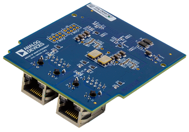
Figure 6 shows a photo of the EVAL-CN0506-FMCZ circuit evaluation board.


Complete information and details regarding the test setup and how to use the EVAL-CN0506-FMCZ can be found in the CN0506 User Guide.