摘要
With the use of proper device initialization and code sequencing, accurate timekeeping and clock alarm operations become a more manageable task.
Introduction
When we read a clock, as we have all done since childhood, our eyes 'take a snapshot' of the present displayed values. Someone has already gone through the effort to reorient that display for your readability. When the microprocessor needs to access the real-time clock, the 'snapshot' of the latest register values must be reoriented into a sequence of time counts that we are more familiar with.
With the use of proper device initialization and code sequencing, accurate timekeeping and clock alarm operations become a more manageable task.
Device Initialization
Upon the first power application to a new clock component, the sequence of required I/O instructions may vary, based upon that specific component. Refer to the device specification for register structuring. As a general guideline, and assuming power is stable and the I/O port is operational, it is recommended to:
- Enable writing to the chip (if a software write-protection option exists)
- Enable the 32kHz RTC oscillator (if not auto-started)
- Define the hardware interrupt output configuration(s) (as applicable)
- Load initial counter values
Enable Writing to the RTC: This unique function was added to some component designs (for example, the DS1305) to prevent inadvertent clock changes. Refer to the product specification for the write-protect (WP) bit explanation.
Enable RTC Oscillator: On some legacy designs (such as DS12887, DS1307), the RTC oscillator does not auto-start at first power-up. This operational feature was intended to prevent battery consumption during transit/storage, and must be enabled through I/O. Designs with an active-low EOSC bit in the Control register include a built-in oscillator auto-start function, executed upon the first power application. In some other designs like DS1685, it may also be necessary to identify the crystal load capacitance setting for proper oscillator operation.
Check 'OSF': Some RTC components contain an oscillator stop flag (OSF), allowing the user to monitor oscillator operation via periodic I/O. Upon initial power application, OSF will be set. After enabling the oscillator, clear OSF, and then periodically verify that the OSF bit remains Logic 0.
OSF may become Logic 1 based upon any of these conditions:
- Initial application of power
- Voltages on VCC and VBAT are insufficient to maintain oscillator operation
- %-overbar_pre%EOSC%-overbar_post% bit was set to 1, stopping the oscillator
- External influences upon the crystal (leakage, coupling, etc.)
Define Interrupt Output(s): Depending upon the specific component and the desired application, definition of the output functions should now be executed to prevent unintended signals from being sent to the microprocessor. Component programming options for real-time alarm(s), watchdog interrupt, square-wave output frequency, etc., should be selected to establish the desired pin/signal conditioning.
In devices with real-time alarms, every alarm register should initially be written to 00h (if binary-coded decimal (BCD)) or FFh (if binary) to prevent any inadvertent matching/interrupt generation. The alarm registers are not factory-initialized, and the associated alarm flags can appear at any time the alarm register contents match the real-time count.
Load Initial Counter (Time) Values: Again referring to the product's specification and register map, the order of counter loading or reading should be executed from least significant count to the most significant count. Figure 1 illustrates the counter orientation and carry functions for a typical BCD-formatted real-time clock component.
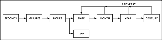
Figure 1. RTC counter chain.
Whenever writing to the RTC, any write to the least significant counter byte resets the internal 1Hz chain, allowing the user one full second before any timekeeping counter bits subsequently increment. This 1Hz reset action, as well as synchronization techniques, are explained in further detail in the Time Synchronization section.
To facilitate ease of use, the registers are oriented in ascending weight and address order for your programming convenience.
| BCD Format | Binary (Seconds) |
| Hundredths of a Second (if so equipped) | 00h -> FFh = 0 -> 255. |
| Seconds | 00h -> FFh = 256. -> 65535. |
| Minutes | 00h -> FFh = 65536. -> 16777215. |
| Hours | 00h -> FFh = 16777216. -> 4294967295. |
| Day of Week | |
| Date | |
| Month | |
| Year | |
| Century (if so equipped) |
Time Synchronization
To some users, the simple act of setting the clock (writing to the RTC) may accomplish the timekeeping accuracy goals for the real-time clock in that application. Depending upon the care taken when initializing our device, an initial clock-set error of a few seconds may be considered acceptable when weighed against the execution of the other tasks controlled by that application.
In other applications, it may be desired to synchronize the real-time clock with a known time standard, like WWV1. As previously mentioned, writing to the least significant counter byte resets the 1Hz countdown chain. Figure 2 illustrates how to reset the 1Hz countdown chain using an I2C Write sequence to the SECONDS register of a DS1340. The slave address byte (D0h), register address (00h), and 'updated Seconds value' (03h), are being transmitted to the component. Two representative examples of an asynchronous 1Hz square-wave output are shown to illustrate the resulting adjustment.
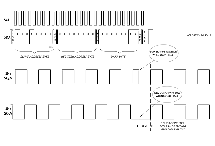
Figure 2. I/O-initiated clock synchronization (I2C format shown).
On the slave's acknowledgement of the data byte (27th rising edge of SCL), the slave simultaneously 1) pulls SDA low to ACK receipt of the data byte, 2) the 1Hz countdown chain is reset, and 3) the new Seconds value (03h in the Figure 2 example) is transferred into the Seconds register.
On the first 1Hz SQW waveform, the 1Hz signal was Logic 1 when the ACK occurred. SQW is immediately pulled low. Precisely 0.5 seconds after the ACK, the SQW output transitions high. Precisely 1.0 second after the ACK, SQW is pulled low, indicating 1 second has elapsed since the write completed. Reading the Seconds register now results in a content of 04h.
On the second 1Hz SQW diagram, the 1Hz signal was Logic 0 when the ACK occurred, so the SQW signal remains low until precisely 0.5 seconds after the ACK, where the 1Hz output will transition high. Precisely 1.0 second after the ACK, SQW is again pulled low, indicating 1 second has elapsed since the write completed. Reading the Seconds register now results in a content of 04h.
For products with 3-wire or SPI I/O, the equivalent trigger to the 27th SCL rising edge in Figure 2 is the next-occurring transition of either SCLK or Chip-Enable (CE or %-overbar_pre%CS%-overbar_post%, whichever input pin naming convention was used).
For products with Phantom I/O, the equivalent trigger to the 27th SCL rising edge in Figure 2 is the termination of the 72nd write cycle in the serial data packet (including the 64-cycle pattern recognition).
For products with Byte-Wide I/O, the equivalent trigger to the 27th SCL rising edge in Figure 2 would be the termination of a write cycle to the Seconds register.
Using Time-of-Day Alarms
On devices with one or more real-time alarm circuits, the user can request either periodic or non-periodic interrupt events to occur at some predetermined time. Alarms can be set up to 30 days in advance of the desired event.
Programming of the alarms suggests use of a few simple rules:
- Initialize all alarm registers to a known state one time (alarms are not POR-reset)
- Never change Real-Time Clock register settings when an alarm circuit is enabled
- Never change Alarm register settings when that alarm circuit is enabled
- Clear the associated Alarm Flag before enabling that alarm (or you may create a premature interrupt)
The most common periodic interrupt is a 'daily alarm', set to activate at 5:30AM, fully independent of the calendar content. To ignore the DAY/DATE register, we will utilize an alarm mask.
Control = 04h			;oscillator on, define %-overbar_pre%INT%-overbar_post%/SQW output function, alarms off
Alarm1 SECONDS = 00h		;0 seconds
Alarm1 MINUTES = 30h		;30 minutes
Alarm1 HOURS = 45h		;5AM in 12hr Mode
Alarm1 DAY/DATE = 80h		;alarm mask set to match on 'Hours, Minutes & Seconds'
Status = 00h			;clear both alarm flags
Control = 05h			;now enable Alarm1 (A1IE=1)
At the next occurrence of 5:30AM, the %-overbar_pre%INT%-overbar_post%/SQW pin will assert.
To clear the interrupt, leaving the alarm enabled for the following morning at the same time, clear the associated Alarm Flag (A1F).
To clear the interrupt and disable any future alarms, clear the associated Alarm Enable (A1IE).
When the associated alarm is disabled, those alarm registers can be used for general-purpose data storage.
Conclusion
Component initialization procedures, when properly sequenced, should include definitions for all of the RTC's hardware functionality required for stable system operation. If desired, the real-time clock can also be synchronized to an external time base, and a procedure for that synchronization has been outlined. Additionally, optional use of real-time clock alarms has been included, focusing upon the order of execution of I/O instructions.
最新视频 21


