Simplifying Your 5G Base Transceiver Station Transmitter Line-Up, Design, and Evaluation
Simplifying Your 5G Base Transceiver Station Transmitter Line-Up, Design, and Evaluation
2024-04-23
摘要
With wireless communication standards such as LTE and 5G, the emphasis on higher data rates and spectral efficiency has driven the wireless original equipment manufacturers (OEMs) to adopt new transmission formats such as orthogonal frequency division multiplexing (OFDM). However, these signals, with large fluctuations in their envelopes, are especially vulnerable to nonlinear power amplifier (PA) distortions due to their high peak-to-average power ratios (PAPR). With this high PAPR signal, a PA nonlinearity can produce substantial signal distortions that increased bit error rates (BERs) and decreased signal-to-noise ratio as a result. This article reviews PAPRs, where they originate, how they can break down the RF components of the transmit line-up, and how to get rid of them or at least mitigate their effects on the signal chain.
Introduction
The newer modulation formats, such as OFDM, and various forms of quadrature amplitude modulation (QAM) have large fluctuations in their signal envelopes. This creates a high PAPR in the signal. Playing a high PAPR signal on a nonlinear PA generates spectral regrowth. Spectral regrowth refers to new frequencies that are caused by gain compression and were not in the original input. The high PAPR causes in-band distortion, which degrades the BER performance of the entire system. We will discuss a solution to help find the right system trade-off between efficiency and linearity using digital predistortion (DPD) and crest factor reduction (CFR) engines.
OFDM Modulation—Everyone Is Doing It!
In LTE and 5G systems, carrier aggregation, which is transmitting several carriers in parallel, is used to increase bandwidth and data rate. These networks leverage OFDM modulation, a very proficient and widely used multicarrier transmission technique that enables better spectral efficiency and reduces the impact of multipath reflections on the receiver’s ability to demodulate the signal. With OFDM, the final waveform is an orthogonal summation of subcarriers that carry information, where each subcarrier has its own center frequency and modulation scheme. In the time domain, sometimes the peaks of these subcarriers can align to produce an aggregate large OFDM waveform peak. A unique feature of OFDM is that the subcarrier waveforms are orthogonally combined such that the null (or zero amplitude) of one subcarrier coincides with the peak of other subcarriers as shown in Figure 1. This provides a relatively efficient use of the channel bandwidth, resulting in improved spectral efficiency compared to traditional single-carrier modulation.

Figure 1. Multicarriers OFDM subcarriers waveforms.
OFDM has several other benefits including its robustness against multipath fading. However, one of the major problems with OFDM modulation is that the transmitting waveforms suffer from a high PAPR. Figure 2 shows the PAPR of various common mobile technologies or modulation types. One can observe that the typical PAPR has been steadily increasing as new standards or modulation technologies have emerged.

Figure 2. Typical PAPR for various modulation technologies.
PAPR in OFDM Signals
As noted, carrier aggregation, enabled by OFDM modulation, is used to increase the bandwidth and data rate in 5G systems. OFDM also results in a signal whose envelope is nonconstant, and this can lead to high PAPR, which can contribute to system damage. If the RF power components in the RF signal line-up, especially the PA, are not suitably specified to handle the expected voltage peaks, these components can fail. A large PAPR reduces the efficiency of the PA by driving it deep into saturation, its nonlinear operating region, leading to distortion that results in spectral spreading of the signal. The linearity of the PA has always been a critical design issue for nonconstant-envelope digital modulation schemes. Figure 3 shows a time domain LTE 64-QAM signal captured at the ADRV9040’s transmitter output.

Figure 3. An illustration of orthogonal summation of subcarriers causing large peaks.
Complementary Cumulative Distribution Function
Due to its form, an OFDM signal requires a statistical approach for proper measurement. The complementary cumulative distribution function (CCDF) is used to evaluate the PAPR reduction performance in an RF signal chain. Figure 4a shows the transmitted waveform of an LTE downlink 10 MHz bandwidth and 64 QAM subcarrier modulation signal. The CCDF in Figure 4b shows that the signal power exceeds the average by at least 7.4 dB for 0.01% of the time. The theoretical maximum peak occurs at 0% probability, which is undefined on this plot. The trace intersects the x-axis (0.01%, or a probability of 10e-4) at a PAPR of about 7.4 dB. This would indicate that one sample out of every 10,000 would be expected to exceed the average power by more than 7.4 dB.

Figure 4. CCDF of an LTE downlink with 10 MHz bandwidth and 64 QAM subcarrier modulation.
Upon taking a closer look at the CCDF graph, observe that the y-axis is cumulative probability and is usually plotted on a log scale; and the x-axis is power plotted in dB. The graph displays the probability or the percentage of time that a signal power is at or above the average power. Essentially, for each power level, the CCDF plot depicts the amount of time the signal spends above the average power level. As the CCDF curve moves to the right, the ratio of our peak power to the average power increases.
The CCDF plot verifies linear operation and is more often measured immediately after a PA. It can give a more accurate depiction of signal compression compared to the commonly used method of tracking changes in gain at differing power levels. The statistical analysis of crest factor occurrence makes it a valuable tool for designers to assess the impact of amplifier compression on the system’s BER and/ or error vector magnitude (EVM).
So, Why Is PAPR Important?
PAs are nonlinear in nature and exhibit a trade-off between linearity and efficiency. The common nonlinear problems are gain compression and phase distortion, including in-band and out-of-band distortions. Each of these factors degrades the BER performance of the system, as well as creates out-of-band spectral regrowth, which leads to adjacent channel interference, and violates out-of-band emissions standards mandated by regulatory bodies.
While testing a PA, the input amplitude is gradually increased until the measured ratio decreases by 1 dB, representing 1 dB gain compression. The 1 dB compression point is a key figure of merit that provides RF designers with assumptions about their amplifier’s performance. Essentially, the 1 dB compression point of an amplifier is defined as the output power at which the device’s gain drops by 1 dB from its small-signal value. This parameter is commonly used as a reference point for the beginning of amplifier nonlinearity and is approximately equal to the maximum useable peak output power for the amplifier. This is why many RF designers typically estimate their PA’s maximum operating output power to be a few dB lower than its 1 dB compression point. This makes finding the 1 dB compression point of a PA a crucial exercise, in order that a signal with a high PAPR is never allowed to saturate the PA. Another name for PAPR is crest factor. Figure 5 shows the AM-AM curve with the 1 dB compression point shown.

Figure 5. The AM-AM curve with the 1 dB compression point.
Now that the designer has evaluated the PA and identified its 1 dB compression point, they need to operate the PA in its linear region with an input power back-off (for example, operate the PA at a lower power within the linear portion of its operating curve) to avoid the spectral growth, right? Well, not exactly!
Simply backing off the input, far from the PA’s saturation point, can certainly help avoid all the nonlinear problems discussed, but results in very low efficiencies and increases heat dissipation. Solving this low efficiency problem by increasing the power consumption of the system is not a viable trade-off. As seen in Figure 2, as the standard bodies got innovative with new modulation schemes to make better use of the existing spectrum, this has resulted in signals with higher and higher levels of crest factor. So, using a PA back off implementation strategy would not work in the long run. The next sections of this article will discuss two implementation strategies that, when combined, will operate the PA up to its saturation point while still maintaining a good linearity and significantly increasing its efficiency. The first uses an amplitude clipping technique for PAPR reduction and the second method is to linearize the nonlinear response of a PA over its intended power range.
The Two Features of a Highly Successful Digital Front-End Solution
In a wireless digital front-end (DFE) system, a broad range of subsystems are covered, including DPD, digital upconversion (DUC), digital down-conversion (DDC), and CFR. There are also other important areas such as DC-offset calibration, pulse-shaping, image rejection, digital mixing, delay/gain/imbalance compensation, error correction, and other relevant blocks. The data captured at the output of the PA is utilized by the DPD circuit to linearize the PA output. DPD improves system linearity by allowing PAs to operate more efficiently, while CFR helps limit the signal PAPR. The DPD engine is used after using CFR to reduce the dynamic range of the signal and allows the PA to be operated above the linear region. While each of these blocks covers key features of the DFE, this section of the article will only focus on the CFR and DPD blocks.
Crest Factor Reduction
Most of the input signal of an OFDM waveform will be within the linear range of the PA. However, as previously shown, the signal has peaks that may exceed the PA’s linear operating range, which invites long-term reliability concerns due to their contribution to system damage. Again, it is highly desirable to drive the PA at the highest input power possible without having it saturate. To avoid saturation due to the peaks, CFR is used, where instead of attenuating the whole signal, only the portions of the signal that are above the PA’s linear range are attenuated. In short, CFR assists in keeping the PA linear.
When peaks are suppressed, this results in a constant output power, thus ensuring that the signal remains within the PA’s linear range. Note that CFR is not a linearization technique, but it is rather an efficiency improvement scheme. With its most effective implementation, CFR eliminates the peaks of the transmit signal to reduce the peak-to-average ratio while complying with the desired spectral emission mask, adjacent channel power ratio, and EVM specifications. Figure 6 shows detected signal peaks above a threshold level. The magnitude of the peaks is reduced to below some target value. This is usually followed by filtering to reshape the signal spectrum.

Figure 6. Detected signal peaks above the threshold level are reduced.
A downside of CFR is that clipping leads to in-band signal distortion, resulting in BER performance degradation, and out-of-band radiation, which imposes out-of-band interference signals to adjacent channels. In short, the consequence of clipping is poor signal ACLR and EVM. Filtering the clipped signal is often used to reduce out-of-band radiation at the cost of peak regrowth.
Digital Predistortion
With DPD, the PA can be pushed to operate up to the saturation region, without compromising its linear characteristics. DPD allows RF designers to operate their systems in the efficient, yet nonlinear, region of a PA while retaining the transmit signal linearity required of the OFDM modulation. In other words, with DPD the PA’s linear region is extended. The DPD engine produces predistorter coefficients by modeling the inverse AM-AM and AM-PM characteristics of the PA. Essentially, DPD focuses on improving the quality of a signal that the PA produces when operating at its peak efficiency point. DPD aims to introduce inverse nonlinearities that compensate for the PA gain. This is a technique for improving the linearity of a nonlinear PA by introducing precise antidistortion into the input waveform that compensates for the PA’s in-band nonlinear products. Figure 7 shows the concept of DPD for linearizing a PA response.

Figure 7. Generic concept of DPD for linearizing the PA response: (a) Typical AM-AM curve showing the overall linear region is in green; (b) basic concept of DPD and how it improves power amplifier efficiency.
It works on the principle of predistorting the transmitted data in the digital domain to cancel the distortion caused by PA compression in the analog domain. The approach to DPD can range from simple solutions such as a basic lookup table (LUT) to a more complex real-time signal processing approach. DPD implementations can be classified into memoryless models and models with memory.
Memoryless DPD
Memoryless DPD corrects the amplitude and phase of the IQ samples based on the current sample only. PAs that are strictly memoryless can be characterized by their AM-AM and AM-PM conversions. This instantaneous nonlinearity is usually characterized by the AM-AM and AM-PM responses of the PA, where the output signal amplitude and phase deviation of the PA output are given as functions of the amplitude of its current input. Therefore, a memoryless PA can be characterized by its AM-AM and AM-PM responses. These measurements are used to create LUT data that relates every input power/phase combination to the power/phase required to produce the desired linear output. The advantage of memoryless DPD is that it can be implemented relatively straightforward as a lookup table. Figures 7a and 7b show AM-AM response of a PA with and without DPD correction applied to a 2× 100 MHz, 400 MHz bandwidth 4096 samples dataset.

Figure 8. AM-AM response of a PA with and without DPD on a 2× 100 MHz, 400 MHz bandwidth signal.
DPD with Memory
As the transmit signal bandwidth gets wider, PAs will begin to exhibit memory effects. These are nonuniform frequency responses in certain components like the biasing network, decoupling capacitors, power supply circuitry, or can be attributed to thermal constants of the active devices. As a result, the current output of the PA then depends not only on the current input but also on past input values. When this is the case, this means that the PA has become a nonlinear system with memory. DPD with memory corrects amplitude and phase of IQ data samples based on several previous samples and their interdependencies. The response of the PA generally does not only depend on the current signal amplitude, but also on the amplitudes of the previous samples. Thus, the digital predistorter would also need to have memory structures—it is the mathematical backbone of DPD. The Volterra series is the most general polynomial type of nonlinearity with memory and used to model nonlinear systems with memory. Therefore, the most general way to introduce memory is to use the Volterra series. For an elaborate discussion on the details of the math behind modeling PA distortion with the Volterra series, which is beyond the scope of this article, please refer to Masterson (2022).2
Framework for Designing 5G RF Signal Chains with Ease
The ADRV9040 RF transceiver provides a streamlined framework for designing, implementing, and testing the RF signal chain lineup of a 5G communication system with ease. A discrete massive MIMO system requires four chip levels in its discrete form of deployment, including an RF transceiver, DFE FPGAs, baseband FPGA/ASIC, and a control FPGA. Since this transceiver comes with the DFE integrated, it eliminates the need for several FPGAs used in competitive discrete solutions where the DPD, CFR, DUC, and DDC blocks are implemented in computer code. The FPGA implementation is typically costly and power hungry. This highly integrated RF transceiver helps eliminate such power-hungry dedicated FPGAs. In this section of the article, we highlight this RF transceiver and a proposed framework for checking a typical PA gain line-up and doing a sanity check for noise limits by implementing register writes inside the device.
This highly integrated, radio frequency agile transceiver system on chip (SoC) offers eight transmitters, two observation receivers for monitoring transmitter channels, eight receivers, integrated local oscillator (LO) and clock synthesizers, and digital signal processing functions to provide a complete transceiver with significant digital front-end capability. The device provides the high radio performance and low power consumption demanded by cellular infrastructure applications such as small cell radio units (RUs), macro 4G/5G RUs, and massive MIMO RUs. The complete transceiver subsystem includes automatic and manual attenuation control, DC offset correction, quadrature error correction, and digital filtering. The transceiver has a fully integrated digital front-end that supports a few key blocks, including DPD (up to 400 MHz IBW), a high performance three-stage CFR engine, integrated digital downconversion and digital upconversion both capable of supporting up to eight component carriers. The device is suitable for such deployments/applications with small cell single-band, multi-band, TDD massive-MIMO, and TDD/FDD in macro-RU equipment. Figure 9 shows a high level functional block diagram.

Figure 9. An ADRV9040 high level functional block diagram.
ZIF-Based Architecture
The transmit and receive signal paths of the ADRV9040 use a zero-IF (ZIF) architecture that provides a wide bandwidth with dynamic range suitable for noncontiguous multicarrier RU applications. The ZIF architecture has the benefits of low power plus RF frequency and bandwidth agility. This architecture provides size, weight, and power advantages over discrete solutions. The architecture enables OEMs to design the smallest and lightest 5G massive-MIMO radios 40% lighter and ~10% more energy efficient. Analysis of a complete small signal radio board shows that the ZIF architecture enables significant cost savings (per 32T32R) on RF BOM vs. simple derivative RUs.
The zero-IF architecture also transmits energy at the LO frequency. The quadrature and LO leakage errors (for example, carriers are not centered on LO) are introduced due to differences in IQ mixing and data paths (for example, two mixers never really have the same characteristics). This is an even bigger issue in multicarrier and asymmetric-carrier applications. To reduce this undesired emission, the transceiver has a Tx LO leakage correction algorithm, which is used both for initial calibration followed by a tracking calibration used during runtime operation.
CFR Block
The device’s CFR assists in keeping PAs linear. This low power CFR engine helps designers reduce the peak-to-average ratio of the input signal, enabling higher efficiency transmit line ups. As mentioned previously, spectral regrowth of corrected peaks is always a concern with CFR. It is crucial to note that the ADRV9040 plays a vital role in optimizing the algorithm to ensure that the impact of the CFR block aligns with the system specifications of the OEM. The ideal CFR block has very low latency and zero missed peaks.
Figure 10 shows the results of a PAPR reduction on a 5G new radio (NR) signal. The pre-CFR (left) plot shows peak compression, which is indicated by the output signal’s CCDF (yellow trace) falling off at a steeper rate than the input, Gaussian reference, CCDF (green trace) as the PAPR increases. On the other hand, the post-CFR (right) plot shows a much improved 5G NR signal where its CCDF is similar to that of the Gaussian signal.

Figure 10. 5G NR signal before and after applying CFR.
This CFR is implemented using a variation of a pulse cancellation technique by subtracting a precomputed pulse from the detected peaks to bring the signal within the PA’s linear range. The CFR block consists of three copies of CFR engines, each of which uses a detection threshold to detect the peaks and a correction threshold to which the detected peaks are attenuated. These spectrally shaped correction pulses are subtracted from the data stream to bring the signal within the PA’s linear range. The correction pulse needs to be spectrally shaped to manage the noise leakage into adjacent bands. The ADRV9040 can hold two correction pulses corresponding to two different carrier configurations on the device at the same time. These correction pulses can be preloaded and allow the device to switch between two carrier configurations on-the-fly.
DPD Block
The device includes a fully integrated, low power DPD engine for use in RF signal chain linearization applications. This engine provides industry-leading DPD performance. As discussed, the most general way to introduce memory is to use the Volterra series. This DPD engine is based on an abbreviated implementation of generalized memory polynomial (GMP) and dynamic deviation reduction (DDR), which are generalized subsets of the well-known Volterra series. The generalized memory polynomials used in the ADRV9040 are discussed in detail in the transceiver’s user guide and other design collaterals. An inverse PA model (PA-1) is applied to the interpolated digital baseband samples through the DPD actuator hardware. A dedicated embedded Arm® Cortex® A55 processor is used for the computation of the GMP coefficients. The DPD actuator is a programmable polynomial calculator. Figure 11 shows a PA-1 model applied to the interpolated digital baseband samples.

Figure 11. An inverse PA model is applied to the interpolated digital baseband samples.
This DPD algorithm supports both indirect learning and direct learning DPD mechanisms for extracting DPD model coefficients. Indirect learning involves using the observation receiver data as a reference for predicting the input samples corresponding to the reference, while direct learning involves using the pre-DPD actuator transmit signal as a reference to minimize the error between the observed and reference data. The difference between the two is that the indirect learning algorithm is time efficient, but the direct learning algorithm is more accurate since it requires a longer time to converge. In a system application where DPD is not needed, the ADRV9040 provides a mechanism to bypass predistortion through GPIO control. Figure 12 shows the power spectral density improvement in ACLR after the application of DPD for a 20 MHz LTE signal. The impairments that provoked the ACLR skirt shown on the left plot have been removed by using DPD on the right plot.

Figure 12. Power spectral density showing improvement in ACLR post-DPD.
Power Management Considerations
Designing the ADRV9040 with the right power solutions is paramount to avoiding issues such as the first symbol poor EVM (for example, Cyclic prefix) at the TDD receive-to-transmit transitions and to achieving optimum RF performance. The ADI Silent Switcher® technology offers several differentiations, including high switching frequency, ultralow rms noise, and spot noise. A Silent Switcher 3 power design requires fewer components, a small PCB footprint (size), and most importantly a faster and well-controlled transient settling time, which results in ultralow EMI emissions. Figure 13 shows a high-level block diagram of a macro base station with a few suggested power ICs, LT8627SP and ADM7172 for powering the ADRV9040 voltage rails.

Figure 13. System-level block diagram of a macro RRH with the ADRV9040 power solutions.
ADS10-V1EBZ and ADRV904X-MB/PCBZ Evaluation Platform
The ADRV9040 evaluation platform facilitates the establishment of a simple and straightforward framework for testing the user’s design. Figure 14 presents the ADS10-V1EBZ (motherboard) and ADRV904X-MB/PCBZ evaluation board. Please contact your ADI sales representative to order your evaluation system. The RF designer only needs to connect his equipment to the eval platform to capture the different plots while the ADRV9040 does the heavy lifting to find the optimal performance configuration via data byte writes into its registers.
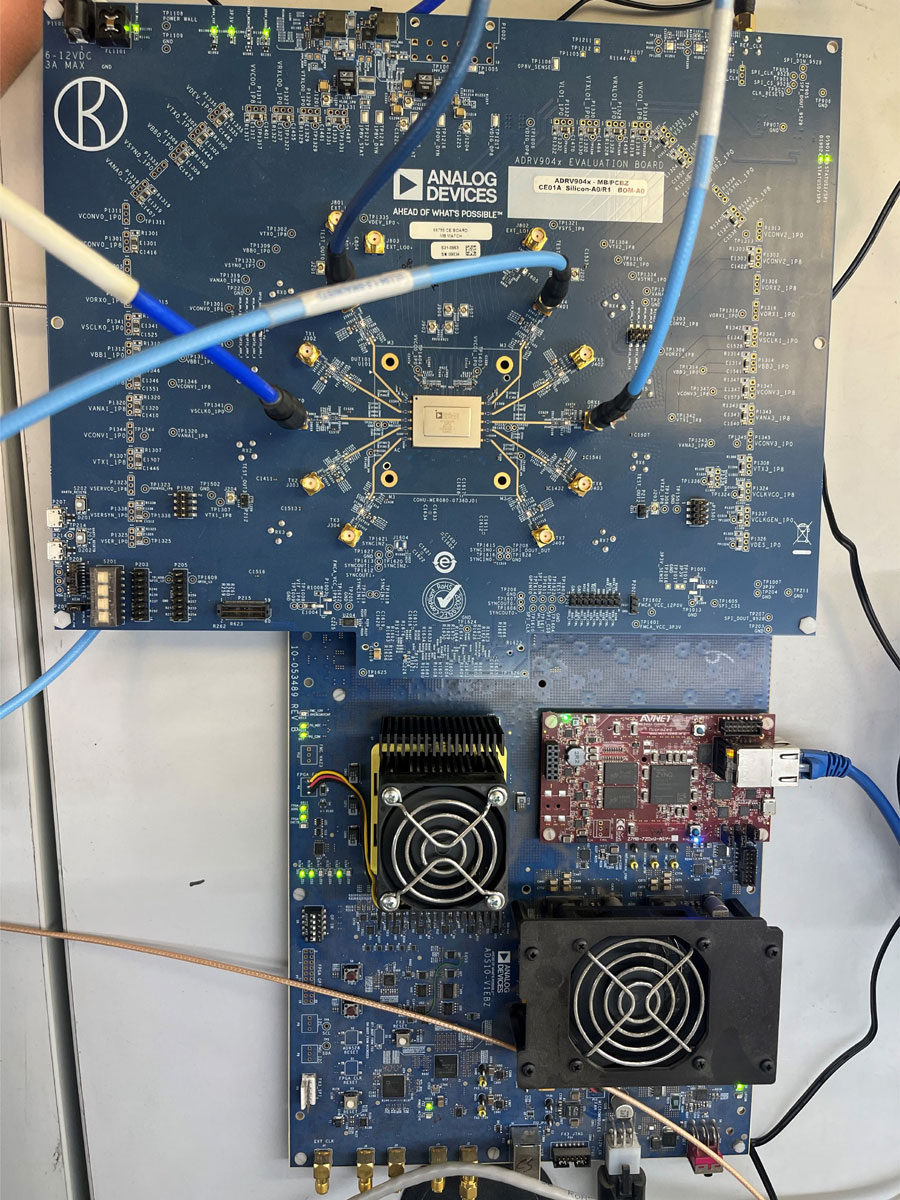
Figure 14. ADS10-V1EBZ (motherboard) and ADRV904X-MB/PCBZ evaluation board.
Conclusion
The advancements in telecom technologies that enable higher data rate communications and improved spectral efficiency through carrier aggregation also contribute to an increase in PAPR. However, by integrating CFR and DPD capabilities into the expertly designed ADRV9040 transceiver, the radio design process is simplified, resulting in reduced RF bill of materials (BOM) cost, board size, weight, and power consumption compared to conventional FPGA-based implementations. With a large number of wireless base stations and remote units deployed globally, improved power amplifier efficiency can significantly reduce energy and cooling costs for service providers. This not only accelerates time-to-market but also helps lower operational expenses (energy and truck rolls) and ensures compliance when deployed in networks.
References
1 “ADRV9040: 8T8R SoC with DFE, 400 MHz iBW RF Transceiver.” Analog Devices, Inc., 2021.
2 Claire Masterson. “Digital Predistortion for RF Communications: From Equations to Implementation.” Analog Dialogue, Vol. 56, No. 2, April 2022.
关于作者
{{modalTitle}}
{{modalDescription}}
{{dropdownTitle}}
- {{defaultSelectedText}} {{#each projectNames}}
- {{name}} {{/each}} {{#if newProjectText}}
-
 {{newProjectText}}
{{/if}}
{{newProjectText}}
{{/if}}
{{newProjectTitle}}
{{projectNameErrorText}}
最新视频 21


