Simple, High Efficiency, Multi-Output, Isolated Flyback Supply with Excellent Regulation
Simple, High Efficiency, Multi-Output, Isolated Flyback Supply with Excellent Regulation
by
Ryan Huff
2006-07-01
Introduction
Simplicity, tight regulation, and high efficiency are no longer optional features in isolated power supplies, but achieving all three is traditionally difficult. High efficiency often requires the use of advanced topologies and home-brewed secondary synchronous rectification schemes. Tight regulation for a multi-output supply is often Simple, High Efficiency, Multi-Output, Isolated Flyback Supply with Excellent Regulation accomplished with inefficient, linear post regulators or efficient (but relatively expensive) switch-mode buck regulator ICs. All of these solutions fail the simplicity test in parts count and design complexity.
Fortunately, a breakthrough IC makes it possible to achieve high efficiency and tight regulation while maintaining the simplicity typically associated with a flyback supply. The LT3825 simplifies and improves the performance of low voltage, multi-output flyback supplies by providing precise synchronous rectifier timing and eliminating the need for optocoupler feedback while maintaining excellent regulation and superior loop response.
48V Input to Triple Output: 5V at 2A, 3.3V at 3A and 2.5V at 3A
The circuit in Figure 1 shows an isolated, no-optoisolator, synchronous flyback, 48V to 5.0V at 2A, 3.3V at 3A, and 2.5V at 3A power supply. Figure 2 shows its efficiency. The converter’s efficiency of over 87% at the nominal input voltage of 48V and full, rated output current on each output approaches that of a higher parts count forward converter. This is primarily the result of a simple, well-controlled implementation of synchronous rectification. As a result of this high efficiency, the greatest temperature rise of any component is only 35°C above the ambient temperature with a paltry 100LFM of airflow.


Figure 1. Simple, high efficiency, 36VIN–72VIN to 2.5VOUT at 3A, 3.3VOUT at 3A, and 5.0VOUT at 2A synchronous flyback


Figure 2. Efficiency of circuit in Figure 1
The feedback winding is used to regulate the output voltage instead of an optocoupler and secondary-side reference, with good results. The regulation curve shown in Figure 3 shows that ±1.6% is easily attainable when loading outputs proportionately. Even when the outputs are loaded in every possible 10% to 100% load current combination, the cross-regulation between all outputs is within ±3.6%. Figure 4 shows the supply’s transient response for a 1.5A-to-3A load step on the 2.5V output at 5A/µs slew rate and 36V input. With this 50% load step, all output voltages remain within ±2% of their set points.


Figure 3. Output voltage regulation of the circuit in Figure 1

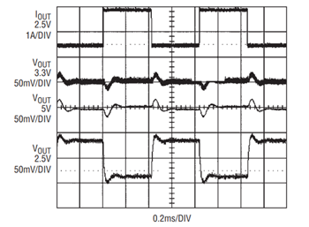
Figure 4. 1.5A to 3A to 1.5A load current step (top trace) on 2.5V output and output voltage responses (bottom traces) of circuit in Figure 1
This circuit also has the advantage of having extremely low ripple on the output voltages; exhibiting less than 10mVP–P on all outputs at a switching frequency of 200kHz. This performance is attributable to the small, second stage, inductor/capacitor filter on each output.
LT3825 Operation
The synchronous rectifier output (SG pin) of the LT3825 makes driving the synchronous rectifier MOSFETs (Q2–Q4) simple while maintaining a low parts count. Setting the dead-time of these synchronous rectifiers relative to Q1 only requires one resistor to program. Avoiding traditional, more complicated, discrete timing circuits allows the designer to set optimum dead-times since this timing is well controlled within the LT3825. The LT3825 also precludes the need for a secondary-side synchronous controller IC and its associated circuitry.
The easy-to-implement synchronous rectification also has another advantage: it tightens the output cross-regulation. An alternative to synchronous rectification is using Schottky diodes, which can vary by more than 0.25V over temperature and load. Under the same conditions, the voltage drop across the MOSFETs in Figure 1 vary only by 60mV, a factor of four better. The MOSFET-based topology tightly couples each output, thereby reducing voltage differences during extreme temperature and cross-loading conditions.
Instead of using a parts-intensive, secondary-side voltage reference and error amplifier to drive an optocoupler, the LT3825 uses the primary bias winding on the flyback transformer, T1 (see Figure 1). The voltage on this winding during the flyback pulse is the average of all output voltages as reflected to the primary. The LT3825 feedback (FB) pin reads this voltage, which is then used to modulate the on-time of Q1 to regulate the output voltages. Cross-regulation performance is enhanced since the average of all outputs is presented to the controller as opposed to just one output voltage’s information as with an optocoupler. Another important benefit of this technique is that the output voltage information arrives at the controller immediately after the switching cycle is terminated. In a conventional optocoupler-based design, delays of tens to hundreds of microseconds occur in the optocoupler alone, severely limiting the converter’s transient response.
Other Features
An optional, resistor programmable, input undervoltage lockout is available. An optional soft-start capacitor controls the slew rate of the output voltage during start-up, which limits the inrush current of the input power supply. Since the LT3825 incorporates current-mode control, both short-circuit behavior and ease of loop compensation are improved over voltage-mode controllers. The switching frequency can be set anywhere from 50kHz to 250kHz, making it possible to find the right balance of solution size and efficiency for a specific application. The switching frequency can be synchronized to an external system clock for further flexibility.
It Is Possible to Reduce the Parts Count Even More
For lower input voltages (5V to 20V) and simpler designs, the LT3837 complements the LT3825. The LT3837 starts up and runs from the lower input voltage connected directly to the VCC pin, so several components are not needed to generate a bias supply, including D1, C6, R1, and R2.
Conclusion
The LT3825 allows a designer to improve the performance of multioutput isolated flyback circuits while lowering parts count and simplifying implementation.
关于作者
关联至此文章
产品
产品分类
{{modalTitle}}
{{modalDescription}}
{{dropdownTitle}}
- {{defaultSelectedText}} {{#each projectNames}}
- {{name}} {{/each}} {{#if newProjectText}}
-
 {{newProjectText}}
{{/if}}
{{newProjectText}}
{{/if}}
{{newProjectTitle}}
{{projectNameErrorText}}
最新视频 21


