Sharing a Reference Can Compromise Precision ADC Performance
Precision ADCs available from Linear Technology offer a high level of performance. In order to attain that high performance many design elements such as a low noise power supply and reference, proper bypassing, a ground plane, a fast settling driver and a low jitter clock must be properly implemented. Poor execution of even one of these elements can seriously compromise the ADC’s performance.
The voltage applied at the ADC reference input is a particularly critical element. Often in an attempt to save money or board space, in a system with multiple precision ADCs, an engineer will be tempted to share a reference in the system without buffering each reference input. The reference pin in ADCs without an internal reference buffer is typically not a static node. As the ADC goes through the conversion process, there will be a series of glitches at the REF pin that must quickly settle in order for the ADC to accurately convert the input signal. If the reference voltage is shared, these glitches can interfere with the conversions of the neighboring ADCs. This can happen even if ADCs of the same type are converting at the same time. The purpose of this article is to show what can happen when multiple precision ADCs share a common reference in order to persuade the reader to avoid this shortcut.
The circuit of Figure 1 shows two LTC2380-24 ADCs connected in chain mode with a common reference. The LTC2380-24 is a low noise, low power, high speed 24-bit successive approximation register (SAR) ADC with an integrated digital averaging filter. The LTC2380-24 has a 145dB dynamic range and can sample up to 2Msps with a typical THD of -117dB. The 47µF reference bypass capacitors are placed as close as possible to the REF pins of the ADCs in an attempt to maximize their effectiveness. Data was taken with the circuit of Figure 1 and with the circuit modified by removing ADC A and grounding the RDL/SDI input of ADC B. The timing is the same for both the one ADC and the two ADC cases to minimize any differences that a change in timing might cause.


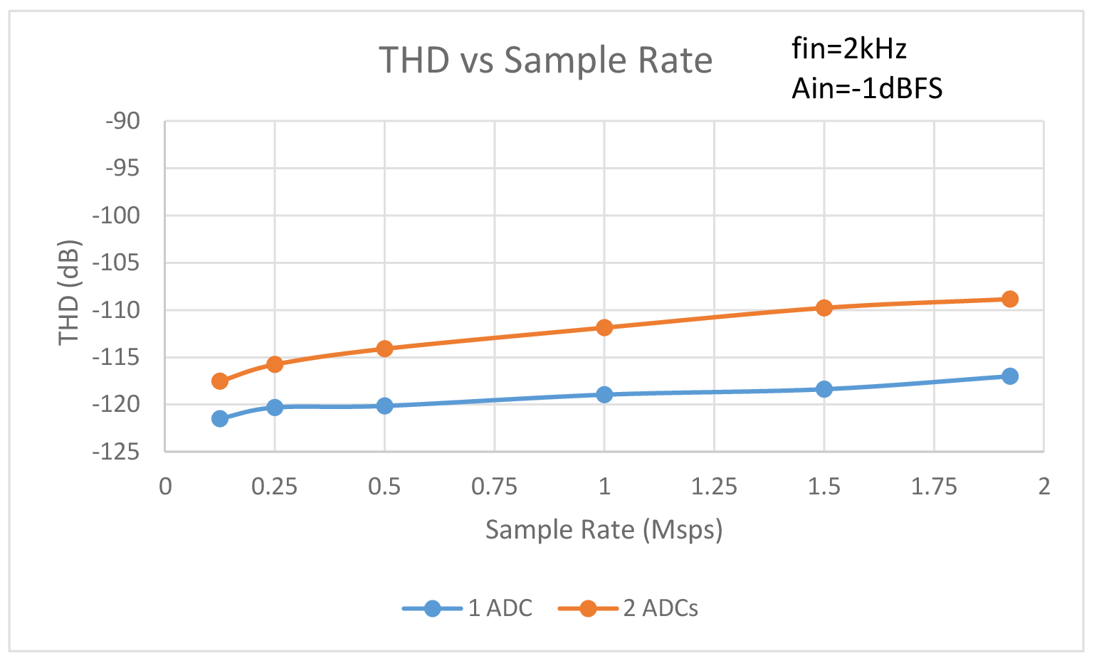
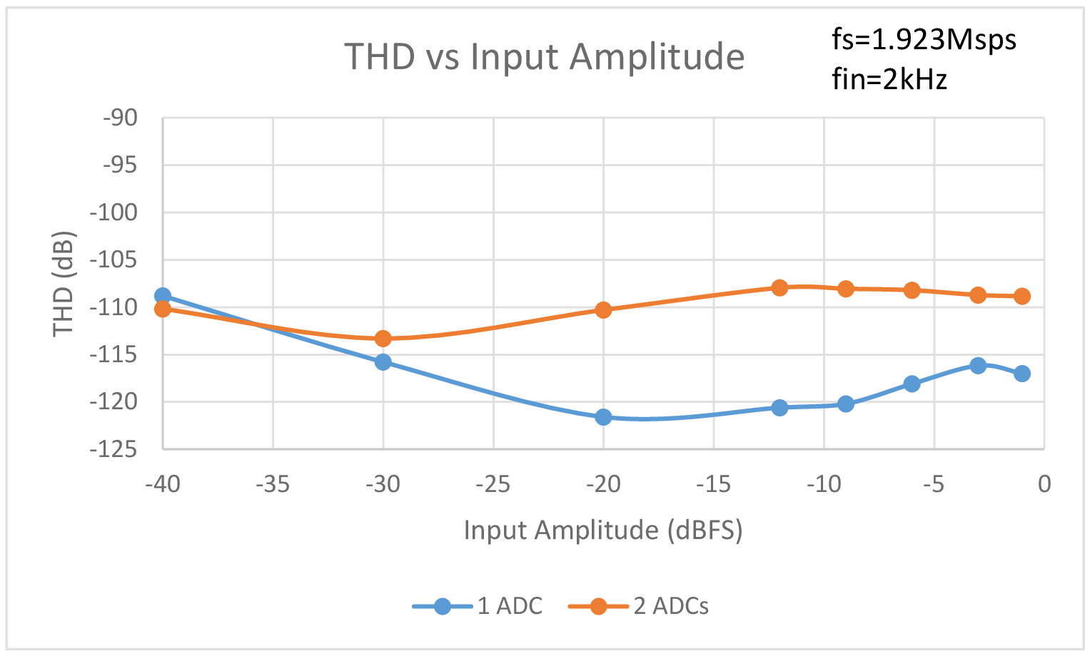
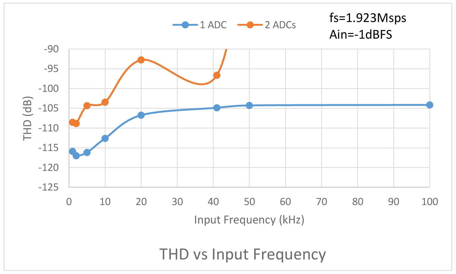
Figure 2 compares THD vs sample rate for one ADC and two ADCs sharing the same reference. As can be seen in Figure 2, sharing the reference causes the THD to drop as much as 8dB at the maximum sample rate. The difference drops to a still significant 4dB with the sample rate slowed to 125ksps. The THD vs input amplitude comparison of Figure 3 shows that sharing a reference causes the THD to drop over 10dB with input amplitudes ranging from -20dBFS to -9dBFS compared to a single ADC. Below input amplitudes of -30dBFS, THD performance is nearly identical. The biggest difference in performance occurs in the THD vs input frequency comparison of Figure 4. Above an input frequency of 41kHz, with 2 ADCs sharing a reference, THD performance starts to go off a cliff. With an input frequency of 50kHz, the THD performance of the two ADCs sharing a reference is literally off the chart at -49dB compared to -104dB with a single ADC. Even at low input frequencies the difference in THD is always greater than 7dB.


The circuit and data presented are intended to demonstrate the loss of performance that occurs when multiple high performance ADCs share the same reference without buffers for each reference input. Significant THD degradation was demonstrated over sample rate, input amplitude and input frequency. After reading this, it is hoped that anyone designing a precision ADC circuit will be persuaded to either use a separate reference for each ADC used or buffer each ADC reference input with a common reference voltage.
关于作者
T他的职业生涯始于LTC,当时的职位是技术员,并向参与多个产品工作的Bob Dobkin、Bob Widlar、Carl Nelson和Tom Redfern学习,涉及产品包括运算放大器、比较器、开关稳压器和ADC。在此期间,他还花了大量时间来编写测试程序以对这些器件的特性进行表征。
关联至此文章
{{modalTitle}}
{{modalDescription}}
{{dropdownTitle}}
- {{defaultSelectedText}} {{#each projectNames}}
- {{name}} {{/each}} {{#if newProjectText}}
-
 {{newProjectText}}
{{/if}}
{{newProjectText}}
{{/if}}
{{newProjectTitle}}
{{projectNameErrorText}}
最新视频 21


