摘要
Article discusses the sources of electromagnetic interference (EMI). It describes how designs with gas arrestors, a varistor, suppressor diodes, chokes and ferrites, capacitors, or series resistors protect equipment. Methods for EMI testing are described.
Introduction
More and more aspects of our lives depend on the uninterrupted operation of electronic equipment and appliances. "Drive by wire" and "fly by wire" have become everyday realities. In automated plants and high-availability systems especially, electronic equipment that fails to operate correctly can cause enormous damage and disruption.
The ideal electronic circuit should be free of active electromagnetic interference (EMI, also called RFI or radio frequency interference) sources and passively immune to disturbances from outside.
The task of minimizing active sources is probably easier than protecting against interference. Common techniques to minimize EMI are line filtering, power-supply design, proper layout, and shielding the enclosure.
Electrical disturbances can be conducted by the power lines or conveyed through the air by capacitive, magnetic, or electromagnetic radiation. Typically, the interference conducted over signal lines connected to the equipment is the most difficult to manage. In any case, one must distinguish between the need to protect against damage or malfunction, and the need to prevent signal or data distortion, for example from a disruption in the sequence of a microcontroller program. The first problem is attacked with hardware design, the second with software algorithms.
This article addresses the means for protecting equipment against the intrusion of harmful voltages and currents.
Guidelines for Regulating EMI
Recognizing the importance of EMI, governmental bodies early undertook the task of enforcing equipment compatibility through regulations. IEC 61000-4, for example, standardizes test methods. Sections relevant to this discussion include IEC 61000-4-2 for electrostatic discharge (ESD), IEC 61000-4-4 for fast transients (FTB), and IEC 61000-4-5 for high-energy transients (SURGE). All of these test methods rely on realistic models for electrical noise.
Before applying any protective elements, consider these basic rules:
- EMI protection should be considered while designing the circuit, not added afterwards.
- Block disturbances as near to the source as possible, preferably before they enter the equipment; redirect them to ground.
- All sections that can be exposed to EMI disturbance, even electrically isolated sections, should be located as far as possible from sensitive circuitry.
Because signal circuitry cannot withstand kilovolt-level voltages, such disturbances must be excluded from the input, converted to current, and then to heat. Ground-loop currents, which can enter an interface and run throughout the circuit, are often thwarted with galvanic isolation. Isolation is especially useful for the longer lines and high ground-loop currents that can occur in industrial systems.
An ESD current pulse of 30A peak may produce only tens of millivolts of resistive voltage drop on a ground trace. However, its extremely steep rise time (> 30A/ns) can induce hundreds of volts of inductive drop on the same trace (assuming roughly 1nH/cm of wire inductance)—more than sufficient to cause data errors. Skin effect applies at these high frequencies; it increases wire resistance dramatically by forcing current to flow only within microns of the conductor surface. To counteract this effect, ground connections need a large surface area to maintain low resistance.
Fast rise times can enable capacitive coupling of FTB and ESD disturbances from noisy sections to supposedly quiet ones. In this context, a frequent mistake is made when designers provide galvanically isolated supplies by adding windings to the main power-supply transformer. This arrangement allows "infected lines" (ground returns for the external signal) to contaminate the entire circuit.
As a compact, functionally clean and cost-effective alternative, you can generate auxiliary voltage at the circuit periphery using a forward converter based on the MAX253 driver. The MAX253 offers a small board space and an effective barrier between the clean and noisy potentials. The tiny transformer required can be manufactured with a coupling capacitance below 10pF, yet it transfers up to 1W while isolating kilovolts (Figure 1).
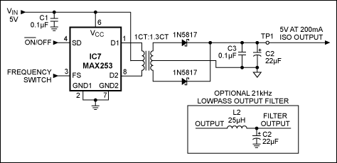
Figure 1. A small transformer and driver IC derives an isolated 5V supply from the 5V rail. For details about 1CT:1.3CT see Table 2 in the MAX253 data sheet.
Other commonly used EMI-protection components are described below.
Gas arrestor is a kind of dish-shaped capacitor filled with gas, frequently neon. Overvoltage in excess of ~100V creates a plasma that limits the voltage at low levels and carries high currents. Gas arrestors absorb high-level transients, but are not suitable for fast transients because the emergence of plasma takes some time. They are not suitable for mains protection and are difficult to use with low-source impedances. Leakage currents in normal operation are very low.
Varistor is an arrestor made with metal oxide (mostly zinc), usually shaped like a tablet with two connectors, one on each side. Behaving similar to a zener diode, a varistor responds much faster than the gas arrestor, but exhibits high leakage currents especially when the signal approaches the clamping voltage.
Suppressor (TransZorb®) diodes are used to limit fast transients at low voltage levels. Their power-dissipation capability is limited according to their form factor. As for varistors, they exhibit significant leakage currents in the vicinity of their breakdown voltage. Junction capacitance is also significant, so in fast systems they are usually decoupled with diode bridges.
ESD structures are novel designs that behave somewhat like diacs. These designs are integrated in the MAX202E, MAX485E, other RS-232/RS-485 transceiver ICs, and recently in analog multiplexers such as the MAX4558. Exhibiting low capacitance and low leakage currents, they are suitable for both ESD and FTB protection.
Chokes, ferrites can attenuate high frequency and fast voltage peaks, but do not absorb much energy. Beware of resonant effects, and always use with attenuating capacitors (commonly an LC filter in a T-structure). An inductor manufacturer usually specifies the self-resonant frequency (SRF). The SRF comes from the parasitic capacitance of an inductor that cancels out the inductance when operating above the SRF. For better performance, use an inductor as an RF choke below its SRF, and never above the SRF. These devices are frequently used to protect against common-mode disturbances and for mains filtering.
Capacitors are perhaps the most important protective element. A capacitor's important features are equivalent series resistance (ESR), inductance, high-current capability, and voltage capability. Proper placement of capacitors in the layout is crucial to minimizing EMI. When used properly, capacitors create a high-frequency ground to from a lowpass filter, bypassing the RF signal to ground. Capacitors also have a self-resonant frequency, a point at which it becomes inductive. Just like an inductor, a capacitor should be used below its SRF. Another way to understand this is to make sure that the SRF is much higher than the frequency of noise that needs to be filtered.
Series resistors are also among the most important and lowest cost protective elements. Properly selected according to resistance and power dissipation, series resistors can replace more costly elements with comparable results.
Good layout design can minimize the effects of EMI. Fast switching currents generate the magnetic field, and fast changing voltages create the electric field that can result in undesired coupling. Electromagnetic coupling can be minimized with the use of good grounds and shield cases. Proper placement of vias is always a good practice. Have multiple vias for bypass capacitors because multiple vias reduce resistance and inductance. Also, avoid a ground that has an unstable ground-voltage potential. Traces that carry high-frequency signals generate a time-varying electromagnetic wave that can propagate the cause of interference. Two traces at a 90-degree angle result in the least interference between the two signals. A good case ground also helps prevent outside signals from entering the system. This, in turn, shields the circuit.
The following examples illustrate use of these components, some working principles, and possible pitfalls.
Thermocouples
Thermocouple signals offer the advantage of quasistatic processing. To guard against signal distortion by ground-loop currents, most thermocouple applications provide galvanic isolation between the signal-acquisition and signal-processing circuitry. As Figure 2a shows, the differential signal is fed through a multiplexer to the input of an instrumentation amplifier, and from there to an analog-to-digital converter (ADC). Opto- or magnetic coupling transfers the ADC's digital output across the isolation barrier.
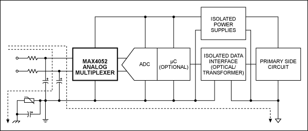
Figure 2a. These components process the differential signal from a thermocouple.
The thermocouple is easily protected with a simple, lowpass RC network of 2kΩ and 100nF on each electrode. An additional 1nF diverting capacitor with high-voltage rating connects the circuit common and the grounded frame of the equipment. This capacitor diverts ESD disturbances to ground while maintaining galvanic isolation for the DC currents. It also forms a capacitive voltage-divider that limits peak voltages at the isolated power supply. To further limit peak voltage, a high-voltage varistor can be connected in parallel with the diverting capacitor (Figure 2b).
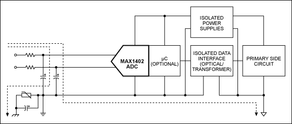
Figure 2b. A high-voltage varistor (lower left) limits the peak voltages.
The 2kΩ resistor must be large enough to withstand high voltage (up to ±8kV ESD, and to dissipate considerable energy during FTB and SURGE testing. Unfortunately, leakage current at the inputs of the following circuit (i.e., before the isolation barrier) can flow through this protective series resistance to create substantial static signal errors. Multiplexers, for example, can introduce unacceptable errors; amplifiers added to buffer the multiplexer can introduce additional input-offset and input-current errors while adding cost and board space to the system.
The MAX4051A multiplexer, which is pin and function compatible with the industry-standard MAX4051, offers a moderate-cost alternative. Its leakage current is guaranteed at 5nA (max) over the extended temperature range and only 2pA typical at +25°C. Thus, the worst-case leakage over temperature at the series resistors creates a maximum error of only 2µV. This error is quite sufficient for most thermocouples. If the application requires even less error, an instrumentation-amplifier buffer based on the MAX4254 quad op amp lowers the leakage to 100pA (max) over temperature and to 1pA (typ) at +25°C. In addition, a low-input offset voltage (VOS) drift (only 0.3µV/°C) makes this buffer extremely effective for high-impedance, low-level signals.
Another alternative is the monolithic MAX1402 signal-acquisition system, which includes a sigma-delta ADC, buffer amplifier, multiplexer, current source for sensor excitation, and so-called burnout current sources for signal validation. It features very low input-leakage current, and the flexibility for implementing applications such as cold-junction compensation.
Angular Encoders
Industrial angular encoders determine the rotor position in electrical machines. Precision positioning systems feature dual-channel, orthogonal, differential sinusoids (called "sincos" signals by some manufacturers).Taken together, these sinusoids form a pointer that allows a fine resolution of rotor position. Alongside the analog-position signal lines, such systems often include RS-422 or RS-485 lines for initializing the encoder and setting its parameters. In some cases these lines run for long distances, carrying analog signals of low-kilohertz frequency and digital data rates as high as megabits per second (Figure 3).
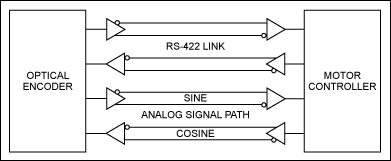
Figure 3. Communication in this optical-encoder system consists of analog "sincos" signals and bidirectional digital-data signals.
Thus, protection in the form of large series resistors and passive RC combinations is excluded, but line-termination resistors (usually 120Ω) are required to prevent reflections. The primary need is for protection against ESD and FTB disturbances. In a system with conventional data transceivers (Figure 4), the differential transmitter's output voltage is limited by a suppressor diode and decoupling diodes. (Decoupling diodes are reverse-biased to decouple the wideband data signal from the capacitance of the suppressor diode, which otherwise would heavily attenuate the signal.)
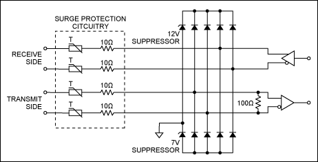
Figure 4. This diode/suppressor network prevents damage from ESD, FTB, and SURGE faults. Optional PTC fuses protect against fault connections to hazardous voltages.
Similar protection is provided for the receiver, but with an important difference: to guarantee an unsymmetrical common-mode range (-7V to +12V for EIA-422A) the limiting network must be unsymmetrical as well. Transmitter outputs and receiver inputs comply with the same common-mode range, so for convenience and economy both are protected by the same suppressor diodes. However, this whole protection network can be replaced by the MAX490E, an RS-422 transceiver that integrates the ESD- and FTB-protection networks.
As a matter of good practice, the transceiver ground should be tied to casing/earth with as short a connection as possible. If the lines are shielded (which is highly recommended!), the shield should also be tied to this point with a short connection. If you expect large exchange currents between separated ground potentials, you should insert a 100Ω series resistor between the shield and earth, preferably bypassed with a low-ESR capacitor.
If the system requires SURGE protection, an external protection network is unavoidable. In that case, it may be advisable to split the line termination so it can function as a current-limiting resistance as well. This is easily accomplished on the receiver side with a moderate loss of signal level. For the driver side, you must verify whether an approximate 10Ω of series resistance is acceptable, given that the MAX490E's differential output impedance is about 40Ω. A possible circuit including PTC fuses in series with the data lines is given in Figure 4 as well.
Standard Signal Interface
The mode of signal transfer chosen for a system is affected by the enormous variety of signal sources and transmission distances which the system may present. For higher bandwidth and longer lines, it is often necessary (especially in systems prone to disturbance) to convert the signals to a higher level: 0V to 10V; -10V to +10V; 4mA to 20mA; or in some cases differential analog, as for an angular encoder. Other systems prefer a digital format carried by wires, optical fiber, or wireless radio links. In all cases, you should minimize noise effects by placing the transducer as close to the signal source as possible.
A ±10V interface, for example, is often used to set the target position in motor-control applications. Those environments are noisy, and the 24V industrial supply (always present in the cabinet) can be a hazard when wiring errors occur. Analog's signal line protectors MAX4506/MAX4507, feature 60Ω channel resistances and a maximum 20nA leakage over temperature. They also offer an elegant protection for this interface (Figure 5). Signals within the supply-voltage range pass through these ICs virtually unaffected.
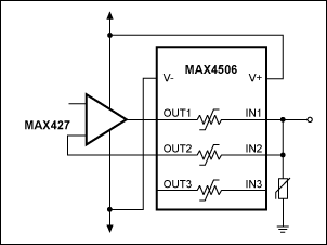
Figure 5. This signal-line-protector IC protects a ±10V interface.
If a disturbance causes the protected terminal signal to exceed the positive or negative supply voltage, the line-protector chip presents a high impedance to the fault signal. It tolerates fault voltages to 36V, or to ±40V with the supplies turned off. Figure 6 shows the input-to-output transfer function for these parts.
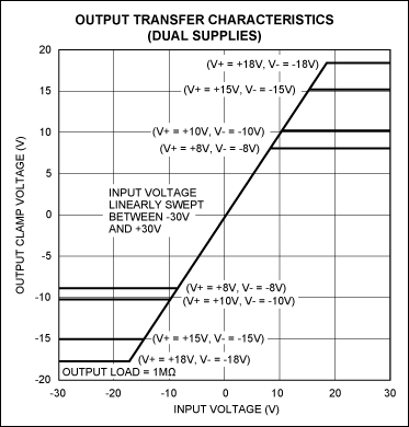
Figure 6. This transfer function illustrates the clamping effect of MAX4506/MAX4507 signal-line protectors.
Using a component such as the MAX4506 or MAX4507, Figure 5 shows a possible protection scheme for ±10V standard signal outputs. The output is generally more difficult to protect than the input, although leakage introduced by protective elements at the input can cause signal errors. It is sufficient to insert a bidirectional suppressor diode, one providing a ±30V clamp voltage, between the line terminal and ground/earth at each receiver input or transmitter output.
Because the suppressor diode's clamp voltage is far beyond the standard signal range, any distorting leakage currents that originate in the suppressor diode are quite low. The line signal is regulated by feedback, while series resistance for the low-signal-line protector places minimum requirements on the driver swing. (It is just 100mV dropout voltage, assuming a 10kΩ minimum load resistance at the receivers.) This protection holds even for continuous faults (to 24VDC, as mentioned above), without endangering either the suppressor diode or the circuit.
Similarly, signal inputs at the receiver side can be protected by inserting a signal-line protector in front of the buffer amplifier. The MAX197, a specialized A/D converter with internal fault protection to ±16V, allows simple and effective protection by connecting bidirectional suppressor diodes (which provide a ±15V clamping voltage) in parallel at the inputs. Software-programmable input ranges for each input channel enable the MAX197 to handle the standard voltage ranges discussed. If higher levels of protection are required, you can place the MAX4507 octal signal-line protector in front of the MAX197.
EMI Immunity Testing and Measuring Techniques
Electrostatic Discharge Immunity Test (IEC 61000-4-2)
The test generator consisted of a high-voltage, 150pF capacitor that discharged through a 330Ω series resistor (Figure 7); a switch; and an electrode, shaped to simulate a finger, that discharged into the equipment under test (EUT).
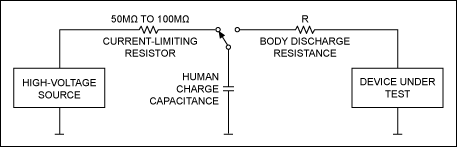
Figure 7. A simple test circuit applies controlled ESD pulses to a test device.
The test specification distinguished between contact discharge and air discharge. Contact discharge was applied by touching the equipment enclosure with the test finger while closing the switch. This procedure exposed the equipment surface to the test voltage (±2kV, ±4kV, ±6kV, and ±8kV), minus a voltage drop caused by current flowing through the series resistor. The resulting short-circuit currents are depicted in Figure 8.
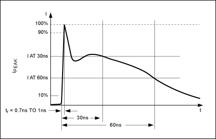
Figure 8. An ESD "zap" from the circuit of Figure 1 produced this current in the device under test (DUT).
Air discharge was applied to insulating surfaces by bringing the test tip toward the surface as rapidly as possible. The test required at least 10 measurements, spaced at least one second apart at each level of standard test voltage (±2kV, ±4kV, ±8kV, and ±15kV). The objective was to find the weakest point within the equipment's enclosure by testing to the limit specified for that class of equipment. Using the same test generator, an additional capacitive-coupling test was implemented by connecting the test tip to a metal plate positioned close (i.e., about 10cm) to the equipment casing. This test applied only to those parts of the equipment that users touch during normal operation and maintenance.
Fast Transient Burst Test (FTB) (IEC 61000-4-4)
An FTB test capacitively coupled a test signal onto the mains line or the signal line. It employed a coupling device that was shaped like a tube and enclosed the line under test for about one meter. The test signal consisted of approximately 75 high-voltage pulses, delivered in bursts at a 3Hz repetition rate. Each pulse had an approximate rise time of 5ns, and a fall time (to 50% of peak value) of 50ns with a 50Ω load or 100ns with a 1000Ω load. The time between pulses was 10µs or 200µs (Figure 9).
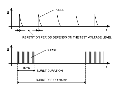
Figure 9. The test pulses in an FTB burst are specified as shown.
To create the high voltage required for low load resistance, the output resistance of this generator was much lower than that of an ESD generator. Peak amplitudes for the test pulses ranged from ±0.25kV to over ±0.5kV, and at a 50Ω load from ±1kV to ±2kV. At 1000Ω the load amplitudes are ±0.5kV, ±1kV, ±2kV, and ±4kV. A decent cable shield, connected properly to ground/earth on the equipment side, can remove a lot of trouble from this test.
SURGE Immunity Test for High-Energy Transients (IEC 61000-4-5)
With considering potential damage hazards to equipment, the most stringent test is for high-energy transients, the SURGE test. In this test, the mains supply lines, unshielded signal lines, or cable shields were driven by low-value series resistors with long-duration, high-voltage pulses. The pulses had approximate 2µs rise times and 50µs fall times (to 50% of peak value); amplitudes ranged from ±0.5kV to ±2kV for mains lines and to ±1kV for signal lines.
For supply lines, the SURGE test galvanically coupled the test signal using a 9µF DC decoupling capacitor in parallel with a series resistance as low as 10Ω (and in some cases, with no resistor at all). Unshielded signal lines were tested with a series resistance as low as 40Ω, line-to-line or line-to-earth. Adding 90V gas arrestors in series prevented capacitive loading of the signal lines between tests (Figures 10a, 10b).
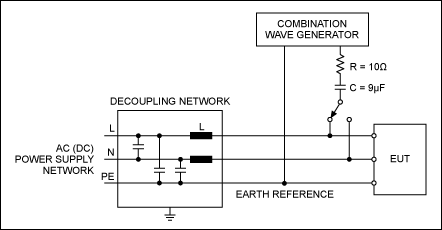
Figure 10a. Test setup: Capacitive coupling of a test signal to AC or DC lines.
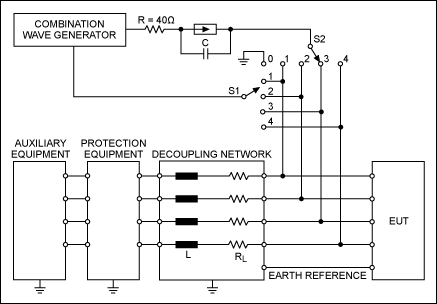
Figure 10b. Test setup: Coupling to unshielded, asymmetrically operated lines.
最新视频 21


