摘要
Field-programmable gate arrays (FPGAs) are used in a wide variety of applications and end markets, including digital signal processing, medical imaging, and high-performance computing. This application note outlines the issues related to powering FPGAs. It also discusses Analog Devices' solutions for powering Xilinx® FPGAs.
Introduction
Field-programmable gate arrays (FPGAs) are used in a wide variety of applications and end markets, and they have been gaining market share over ASICs due to their excellent design flexibility and low engineering costs. Power-supply design and management for FPGAs is an important part of the overall application. This article discusses ways to overcome some of the power-supply design challenges and explains the trade-offs between cost, size, and efficiency. Analog Devices' solutions for Xilinx FPGAs are also presented.
FPGA Overview
FPGAs are programmable devices consisting of an array of configurable logic blocks (CLBs) connected through programmable interconnects. These CLBs typically comprise various digital logic components, such as lookup tables, flip-flops, multiplexers, etc. Other components of an FPGA include input/output pin driver circuits (I/Os), memory, and digital-clock management (DCM) circuits. Modern FPGAs integrate features that include FIFO and error correction code (ECC) logic, DSP blocks, PCI Express® controllers, Ethernet MAC blocks, and high-speed gigabit transceivers Figure 1.
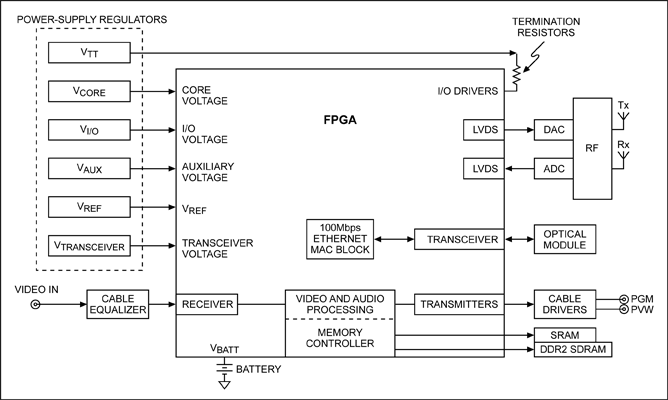
Figure 1. A typical FPGA application block diagram.
System-Level Power-Supply Architecture for FPGA Applications
Most high-performance/high-power FPGA applications in communications applications are built on plug-in cards that are powered by a 48V backplane. A two-stage intermediate bus architecture (IBA) is typically used in these applications for the individual cards (Figure 2). The first stage is a step-down converter that converts the 48V to an intermediate voltage, such as 12V or 5V. The plug-in-cards are often isolated from each other for safety reasons, and to eliminate the possibility of current loops and interference between the cards. The second stage of the IBA is to convert the intermediate voltage to multiple lower DC voltages, using nonisolated regulators known as "point-of-load" (POL) regulators. FPGAs used in computing, industrial, and automotive applications typically derive their power from a 12V to 24V nonisolated supply.
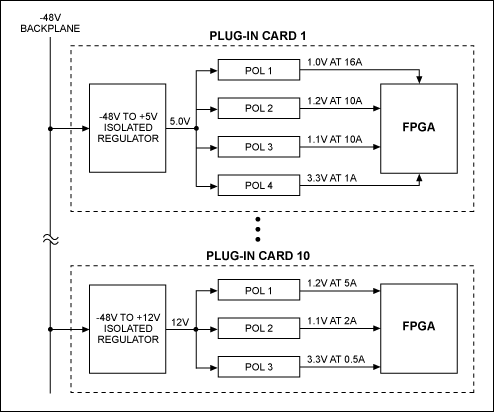
Figure 2. Typical 2-stage intermediate bus architecture (IBA) for FPGAs.
POL Regulators
POLs are high-performance regulators whose VOUT rails are placed close to their respective loads. This helps solve the difficulties of high-transient-current demands and the low-noise requirements of high-performance semiconductor devices like FPGAs. The application-level parameters to be considered when designing a POL are:
- Cost
- Size
- Efficiency
The priority assigned to each of the above parameters often depends on the end market. Thus, each solution should be considered independently. For example, industrial and medical markets tend to favor size over cost, while wireless applications generally favor cost over size. Consumer applications are very conscious of all three parameters. Efficiency is particularly important to applications that run on batteries. The required efficiency usually determines what kind of DC-DC regulator is used, either low-dropout linear regulators or switch-mode power supplies.
Low-Dropout Linear Regulators (LDOs)
LDOs are relatively simple to implement, inexpensive, and produce very little noise. The major drawback with LDOs is their poor efficiency, which depends on the ratio of VOUT to VIN. For example, an LDO with VIN = 3.3V and VOUT = 1.2V has only 36% efficiency. The power difference is dissipated as heat.
Switch-Mode Power Supplies (SMPS)
SMPSs are typically > 90% efficient but are more difficult to implement than LDOs. They also conduct and radiate more noise when compared with LDOs.
LDOs are typically considered for applications with relatively low power requirements. SMPSs are used in higher-power applications due to their better efficiency, an important parameter for thermal management and reliability. Higher efficiency results in lower device temperatures, which improves reliability and reduces the overall solution size through smaller heatsink requirements.
Typical FPGA Power Requirements
A good example of a high-performance FPGA is the Xilinx Virtex®-7 FPGA. Table 1 shows the main voltage-supply requirements for this part. There are also other less-demanding voltage rails such as VCCBRAM, VBATT and VREF that require lower current levels. In many applications, a single power supply can be used, along with passive filters to supply two or more of the power rails that use a common voltage. In these cases, the power supply may be required to supply 20A or more.
| Power Rail | Nominal Voltage (V) | Tolerance | Description | |||
| VCCINT | 1.0* |
±3%* | Voltage supply for the internal core logic | |||
| VCCAUX | 1.8 | ±5% | Voltage supply for auxiliary logic | |||
| VCCO | 1.2 to 3.3 | 1.11V to 3.45V** | Voltage supply for I/O banks | |||
| MGTAVCC | 1.0 | ±3% | Voltage supply for GTX transceiver | |||
| MGTAVTT | 1.2 | ±30mV | Voltage supply for GTX transceiver termination circuits | |||
| *The lowest-speed "-1L" version of the Virtex-7 has a 0.9V core voltage with a ±30mV tolerance. **The specification for 3.3V HR I/O banks is 3.45V (max). The specification for 1.8V HR I/O banks is 1.89V (max). |
||||||
| Power Rail | Description |
| VCCINT | Voltage supply for the internal core logic: supplies power to the internal logic functions, such as CLBs, block RAM, and DSP blocks. |
| VCCAUX | Voltage supply for auxiliary logic: supplies power to the various auxiliary circuits, such as clock managers and dedicated configuration pins. |
| VCCO | Voltage supply for I/O banks: powers the output buffer drivers. |
| MGTAVCC | Voltage supply for the GTX transceiver: powers the internal analog circuits of the GTX transceiver. This includes analog circuits for the PLLs, transmitters, and receivers. |
| MGTAVTT | Voltage supply for GTX transceiver termination circuits |
FPGA manufacturers such as Xilinx have power estimation spreadsheets for estimating the power requirements of an FPGA device, based on the required functionality of the FPGA (www.xilinx.com/power). Designers should use these spreadsheets at the early design stage of a project to assist in selecting appropriate power-supply and thermal-management components. Through the use of the power estimators, designers can determine the voltage supply rails needed and their currents to select the most suitable regulators. Table 2 shows a sample power budget for a Virtex-7 FPGA. These power calculations are used to determine the system efficiency and the required thermal-management solution.
| Regulator | VOUT (V) | IOUT_MAX (A) | POUT (W) | VIN (V) | Efficiency (Estimated) | PIN = POUT/Eff. | IIN Required (A) | Power Dissipated (W) |
| VCCINT | 1.0 | 3.0 | 3 | 5.0 | 0.95 | 3.16 | 0.63 | 0.16 |
| VCCAUX | 1.8 | 1.0 | 1.8 | 5.0 | 0.92 | 1.95 | 0.39 | 0.15 |
| VCCO | 1.5 | 0.3 | 0.45 | 5.0 | 0.91 | 0.494 | 0.1 | 0.044 |
| MGTAVCC | 1.0 | 3 | 3 | 5.0 | 0.92 | 3.26 | 0.65 | 0.26 |
| MGTAVTT | 1.2 | 2 | 2.4 | 5.0 | 0.91 | 2.64 | 0.53 | 0.24 |
| Total | 10.65 | 11.50 | 2.3 | 0.85 |
Power-Supply Considerations
In addition to using the power estimation tools to estimate the FPGA supply rail voltages and currents, there are several other aspects to choosing a power regulator. The following are some topics to consider.
Startup Sequencing/Tracking
Three or more voltage rails are typically required to power an FPGA. It is good design practice to implement sequencing for power-up and power-down between these rails. One advantage of this is that sequencing limits the inrush current during power-up. Also, even if the FPGA itself does not require sequencing, other devices in the design, such as microcontrollers and flash PROM, may have sequencing requirements. If the sequencing is ignored, the devices that require sequencing can be damaged or latchup which, in turn, can cause a malfunction.
There are three types of sequencing:
- Coincident tracking (also known as "simultaneous tracking")
- Sequential
- Ratiometric tracking
Figure 3 shows the different sequencing types and how the voltage rails rise in relation to each other.
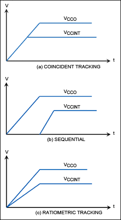
Figure 3. The three types of sequencing: (a) coincident tracking, (b) sequential, and (c) ratiometric tracking.
With coincident tracking, typically the preferred sequencing method for FPGAs, the rails ramp up simultaneously and at the same rate to their final set-points. This prevents unreliable startup due to latchup and bus contention. It also avoids turning on any parasitic conduction paths that could damage an FPGA. The higher startup inrush currents required by this type of sequencing can require a larger capacitor bank to ensure that the rails rise monotonically. The inrush current issue is alleviated by the adjustable soft-start feature found on most of Analog's POLs. For example, the MAX8686 facilitates coincident tracking and provides a programmable soft-start time based on the value of a single capacitor.
The main advantage with sequential sequencing is that it is generally easy to implement; startup inrush-current requirements are less than both coincident and ratiometric sequencing. However, the maximum voltage differential occurs between the voltage rails with this method, which could cause unreliable device behavior.
Ratiometric tracking ramps up all the voltage rails to reach their set-points at the same time. This reduces the voltage differential between the rails, compared to sequential sequencing. The level of startup inrush current is between the level for coincident tracking and sequential sequencing.
Monotonic Startup Voltage Ramping
It is important for the ramping voltage rails to rise monotonically at startup to achieve successful power-up. That means that they should rise continuously to their set-point and not droop. Drooping could result if the POL does not have enough output capacitance (Figure 4). The critical area for most FPGA core voltages is between 0.5V and 0.9V when the internal logic blocks are initialized to valid operating states.
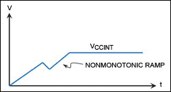
Figure 4. Example of nonmonotonic voltage ramp at startup.
Soft-Start
Most Xilinx FPGAs specify minimum and maximum startup ramp rates of 0.2ms and 50ms, respectively. However, there are exceptions. For example, the "-1L" version of the Spartan®-6 ramp rate is 0.2ms to 40ms, while the Spartan-3A has a ramp rate of 0.2ms to 100ms.
Power-supply regulators implement soft-start by gradually increasing the current limit at startup. This slows the rate of rise of the voltage rail and reduces the peak inrush current to the FPGA. Analog's POLs allow soft-start times to be programmed based on the value of a soft-start capacitor connected to one of the POL pins.
Prebiased Startup
There are situations where an FPGA voltage rail remains biased at some voltage level when a power supply is shut down. This prebias is usually the result of various parasitic conduction paths through the FPGA. If the power supply restarts and pulls the prebiased output voltage low, it can result in unsuccessful startup of the FPGA. The output voltage of the power supply should instead be ramped up to its set-point, along with the other FPGA voltage rails in their desired sequence.
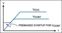
Figure 5. Recommended sequential sequencing startup for a prebiased output.
PCB Layout
While working on the PCB design, engineers must consider component placement, signal routing, and board layers. A multilayer board is highly recommended for FPGA designs, with a ground layer between each signal routing layer. The shielding that the ground layers provide allows for signal routing on every layer, without having to consider the adjacent routing layers. This facilitates a simpler and more practical layout.
Power-supply voltage and ground-plane placement in the PCB layer order (stackup) have a significant impact on the parasitic inductances of power current paths.
- High-priority voltage-supply layers should be placed closer to the component layer (in the top half of the PCB stackup). For example, power supplies with high-transient currents should have their associated voltage and ground planes close to the component layer. This decreases the via length (parasitic inductance) through which the high-transient currents must flow.
- Low-priority supplies should be placed farther from the component layer (in the bottom half of the PCB stackup).
Decoupling capacitors should be connected as close to the FPGA power pins as possible. The decoupling capacitors reduce any conducted noise from the power supply and radiated noise from surrounding circuits.
Some recommendations for the SMPS layout are:
- Minimize any parasitic inductance in the power-supply switched-current path by using short and wide traces between the critical components. This reduces the magnitude of voltage spikes that can be conducted and radiated into the FPGA.
- Place the regulator's decoupling capacitors as close to the regulator's IC pins as possible. Separate the power and analog ground planes.
- Keep the traces from the regulator's gate driver pins to the MOSFET gate pins short and wide to reduce the impedance seen by the gate-drive current.
- The high-current power-supply components that connect to the inner ground plane should use many ground vias to reduce the loop impedance.
See the MAX8686 data sheet for more layout information.
Power-Supply Transient Response
FPGAs can implement many functions at different frequencies due to their multiple clock domains. This can result in larger step changes in current requirements. The term "transient response" refers to a power supply's ability to respond to these abrupt changes in load current. A regulator should respond without significantly overshooting or undershooting its set-point and without sustained ringing in the output voltage. The transient response of a regulator depends on the following:
- The speed at which the regulator's control loop responds when it detects a change in output voltage (or current, in the case of a current-mode controller).
- The value and quality of output capacitance.
The control-loop unity-gain crossover frequency is typically designed to be 1/10 the regulator switching frequency. Thus, the regulator can be designed to respond quickly by operating at a high switching frequency (~1MHz).
The output capacitors should have very low effective series resistance (ESR) and be large enough to minimize the magnitude of the VOUT transient overshoots and undershoots. Polymer capacitors provide the most capacitance with the lowest ESR. Ceramic capacitors have excellent high-frequency characteristics, but their total capacitance per device is one-half to one-quarter that of polymer capacitors. Typically, polymer or tantalum capacitors are used for the bulk output capacitance, while relatively low-value ceramic capacitors are placed at the FPGA input power pins for final stage filtering (Figure 6).
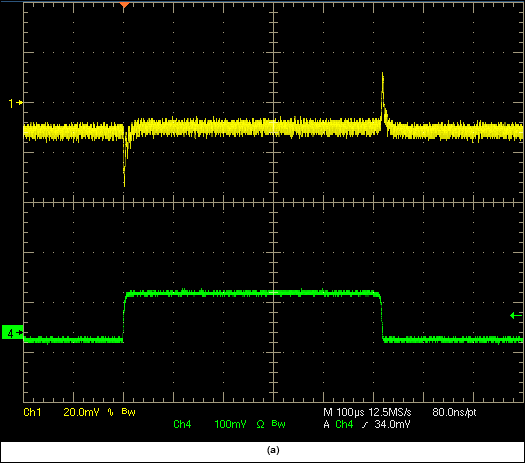
Figure 6. A 12VIN, 1.2VOUT-at-20A, 2-phase MAX8686 power-supply design for the Virtex-6 GTX transceiver. (a) Transient response: 2A-to-12A load step with 22mVOUT transients.
 IN, 1.2VOUT-at-20A, 2-phase MAX8686 power-supply design for the Virtex-6 GTX transceiver. (a) Transient response: 2A-to-12A load step with 22mVOUT transients. (b) VOUT ripple < 5mV at 5AOUT." class="img-responsive">
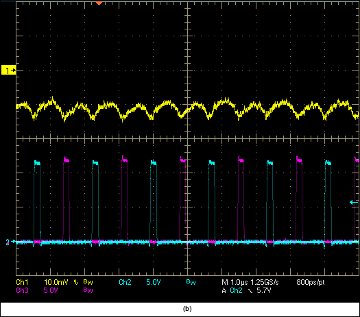
Figure 6. A 12VIN, 1.2VOUT-at-20A, 2-phase MAX8686 power-supply design for the Virtex-6 GTX transceiver. (b) VOUT ripple < 5mV at 5AOUT.
Synchronizing to an External Clock
FPGAs applications usually require the power regulators to synchronize to a common clock. Many POLs provide an external SYNC pin to allow the system designer to synchronize one or multiple regulators to a common system clock.
Multiphase Operation
Multiphase regulators are essentially multiple regulators operating in parallel with their switching frequencies synchronized and phase shifted by 360/n degrees, where n identifies each phase. The advantages of designing with multiphase regulators become apparent as load currents rise above 20A to 30A. These advantages include:
- A reduced input-ripple current, thus significantly decreasing the required input capacitance.
- A reduced output-ripple voltage due to an effective multiplication of the ripple frequency.
- A reduced component temperature, achieved by distributing the losses over more components.
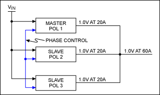
Figure 7. Multiphase regulator block diagram.
Remote Sensing
There can be a significant voltage drop between the power-supply output and the FPGA power-supply pins. This occurs particularly in applications where the load current is high and it is not possible to place the regulator circuit very close to the FPGA power pins. Remote sensing resolves this issue by using a dedicated pair of traces to accurately measure the voltage at the FPGA's power-supply pins (Figure 8). Remote sensing is also recommended for voltage rails with very tight tolerances (≤ 3%).
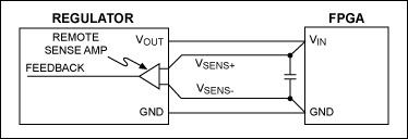
Figure 8. Remote-sensing block diagram.
Analog Devices' Power Solutions for Xilinx FPGAs
Analog provides both LDO and SMPS regulators. SMPS regulators are typically selected to supply the higher power FPGA voltage rails: The SMPSs produce better system efficiency and thermal management. Analog's SMPS regulators offer a complete power-management solution where performance, power density, quality, and digital power management with accurate monitoring and control are required.
Analog's power regulators include:
- PWM controllers
- PWM regulators—controllers with integrated MOSFETs and/or internal compensation and digital programming capability
- PMBus™ digital system control and monitoring
- Digital power control ICs
Synchronous PWM Controllers
Synchronous PWM controllers replace the external Schottky diode with a MOSFET to implement synchronous rectification, which improves efficiency. Synchronous PWM controllers can handle high current levels, since the switching MOSFETs are external to the controller ICs. Designers can select the most appropriate discrete MOSFETs for their particular current requirements.
Analog provides a variety of synchronous PWM controllers for use with FPGAs. For example, the MAX15026 is a single controller, the MAX15023 is a dual controller, and the MAX15048/MAX15049 are triple controllers, all of which operate at up to 28VIN, making them suitable for 5VIN and 12VIN FPGA applications. Analog also provides higher-voltage controllers (up to 40VIN), such as the MAX15046, for industrial and automotive applications. Most of Analog's dual (or higher) controllers also have built-in sequencing and tracking that allow designers to use multirail ICs without requiring external sequencers.
PWM Regulators
Analog's selection of PWM regulators facilitate output currents from 1A to 200A with input voltages ranging from 2.5V to 28V. All regulators have switching MOSFETs integrated with the PWM controllers. Examples include the MAX15053, MAX15041, and MAX8686. The MAX15021 and MAX17017 are multirail regulators that support dual and quad supply rails. Many of these ICs have popular fixed output-voltage options with fully internal compensation.
Some parts support digital programming, optional digital control, and monitoring functions that allow microsecond resolution programming of all timing events, such as sequencing and tracking. These extremely flexible monitoring features allow for intelligent settings of warning and fault thresholds. Independently setting the fault-handling scenario for each regulator is also facilitated. Fine control of the output voltage with 0.2% accuracy will ensure meeting the tight tolerances of high-end FPGAs. Digital programmability and monitoring make field updates possible with a remote connection, and that helps avoid expensive field servicing. Additional benefits include the ability to log events so that failures can be studied and the root causes identified. A more comprehensive list of Analog's POL regulators is given in our product guide, Analog Solutions for Xilinx FPGAs.
POL Digital System Control and Monitoring
Rack-based infrastructure equipment in communications and computing applications require sophisticated power management to turn on/off supplies and fans. Several customers building equipment for these markets use the Power Management Bus (PMBus™) protocol. The PMBus is an open-standard power-management protocol with a fully defined command language that facilitates communication with power converters and other devices in a power system. Analog provides several PMBus monitors and system controllers. The MAX34440/MAX34441/MAX34446 are good examples of complex system PMBus monitors. These devices monitor the power-supply output voltages and constantly check for user-programmable overvoltage and undervoltage thresholds. The MAX34440 can manage up to six power supplies (Figure 9). The MAX34441 can monitor up to five power supplies and also contains a closed-loop fan-speed controller. Both the MAX34440 and MAX34441 can margin the power-supply output voltage up or down to a user-programmable level. The margining is performed in a closed-loop arrangement, whereby the device automatically adjusts a pulse-width-modulated (PWM) output and then measures the resultant output voltage. The power-supply managers can also sequence the supplies in any order at both power-up and power-down. With the addition of an external current-sense amplifier (CSA), these devices can monitor currents.
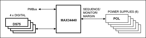
Figure 9. The MAX34440 PMBus 6-channel power-supply manager.
The MAX34446 power-supply data logger monitors voltages for overvoltage and undervoltage, as well as for overcurrent and overtemperature conditions. The device constantly checks for user-programmable thresholds; when these thresholds are exceeded, the devices log the recent real-time operating conditions in nonvolatile flash memory (Figure 10). The devices can monitor up to four voltages or currents, and can monitor three temperature sensors.
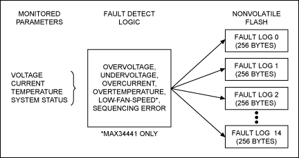
Figure 10. MAX34440/MAX34441/MAX34446 fault detection/logging.
The MAX8688 is an example of a fully integrated, digital power-supply controller and monitor that operates with any existing POL to provide complete digital programmability (Figure 11). By interfacing to the reference input, feedback node, and output enable, the MAX8688 takes control of the POL to provide functions such as tracking, sequencing, margining, and dynamic adjustment of the output voltage.
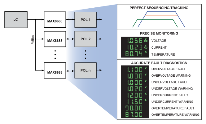
Figure 11. The MAX8688 digital system control and monitoring of POLs.
Digital Power-Control ICs
Historically, power-supply companies have focused on LDO and SMPS regulators. However, in complex infrastructure equipment that uses system-level power management, a more advanced digital control loop promises automatic compensation that is independent of output voltage. This advanced digital control loop results in design simplicity and dynamic power management. Unlike typical power regulators that use the analog control loop, digital power-control ICs (DPCs) use digital circuits to implement the control loop of a power supply. Customers requiring advanced system power management can benefit from a total solution cost advantage. Like the analog power regulators reviewed before, these DPCs have also integrated on-chip digital power-management functionality that communicates to a system controller over the PMBus interface, facilitating easy power-supply design through a graphical user interface (GUI). The digital control loop ICs promise several benefits:
- Shorter Time-to-Market: Sophisticated DPCs can reduce design time by automatically compensating the control loop irrespective of output voltage. For customers who already benefit from internally compensated POLs with analog control, digital control takes it to the next level of ease of use.
- Lower Cost: DPCs decrease the number and size of components. The output capacitors can be reduced by up to 50%. Reliability is improved through the use of fewer components.
- Improved Performance and Reliability: The response to IOUT transients is optimally controlled, resulting in lower VOUT transients. The control algorithm improves efficiency by adjusting to voltage, current, and temperature variations.
- Enhanced Flexibility: DPCs simplify the system power-supply management. The system power supplies are controlled through the PMBus and additional power supplies can be easily added or removed for future system designs.
InTune™ Digital Power
Analog's InTune digital-control power products make it easy to achieve high-performance, DC-DC power-supply designs that require less filter capacitance and have greater efficiency. InTune digital power technology is based on "state-space" or "model-predictive" control, rather than the proportional-integral-derivative (PID) control used by competitors. The result is a faster transient response. Unlike competing PID controllers, the InTune architecture uses a feedback analog-to-digital converter (ADC) that digitizes the full output voltage range, thereby eliminating the compromise associated with "windowed" ADCs used in competing controllers. Its automatic compensation routine is based on measured parameters providing better accuracy and efficiency over a wide range of operating conditions.
The MAX15301 in Figure 12 is a full-featured, flexible, and efficient digital POL controller based on InTune architecture with advanced power-management and telemetry features.
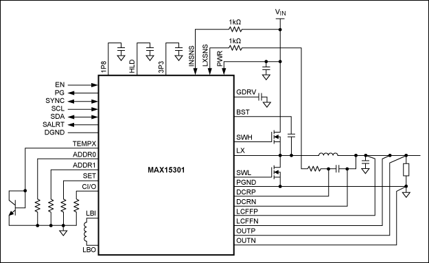
Figure 12. The MAX15301 typical operating circuit.
Analog Devices Reference Designs for Xilinx FPGAs
Analog has built several reference designs for Xilinx FPGAs and CPLDs representative of several end markets and applications. Examples include designs featuring the entire spectrum from high-end Virtex Series FPGAs using several multigigabit transceivers (GTP/GTX) to low-power CoolRunner-II CPLDs. Some of the reference designs are discussed below. Analog's FPGA power team is available to help with example designs to help customers. Contact your sales representative for getting access to the hardware and reference designs.
Analog GTX and GTP Power Modules for the Virtex-6 GTX and Spartan-6 GTP Transceivers
Analog has 10Gbps GTX and 3.125Gbps GTP power modules to power Xilinx ML623 and SP623 transceiver characterization kits. Based on the MAX8686, these power modules operate from 12VIN (±10%) and power the MGTAVTT and MGTAVCC rails of Virtex-6 GTX and Spartan-6 GTP transceivers. Since the GTP and GTX transceivers run at high line rates, a poor switching power supply can impose noise on the data eye. Analog's power modules have a very low noise profile and display superior soft-start and output-voltage ripple compared to competing solutions.
The GTX module produces:
- 1.025V at up to 20A for powering the MGTAVCC voltage rail.
- 1.2V at up to 20A for powering the MGTAVTT voltage rail.
The GTP module produces:
- 1.2V at up to 20A for powering the MGTAVCC voltage rail.
- 1.2V at up to 20A for powering the MGTAVTT voltage rail.
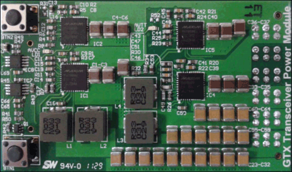
Figure 13. A 2-phase MAX8686 power supply for the Xilinx Virtex-6 GTX transceivers for use with the Xilinx ML623 board. A similar board is available for the Xilinx Spartan-6 GTP transceivers for use with the Xilinx SP623 board.
The MAX8686 current-mode, synchronous PWM step-down regulator with integrated MOSFETs operates from a 4.5V to 20V input supply and generates an adjustable output voltage from 0.7V to 5.5V. The adjustable switching frequency of the MAX8686 is set to 550kHz for an optimal trade-off between component size and efficiency. The programmable soft-start is set to 1ms to meet the FPGA's specifications. The output voltage rails start up monotonically even when a prebias output voltage is present. The MAX8686 also facilitates startup sequencing between the output voltage rails, while a hiccup current-limit feature reduces the power dissipation during short-circuit conditions.
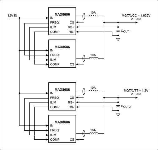
Figure 14. Block diagram of the Analog power module for the Xilinx Virtex-6 GTX transceiver. The block diagram for the Spartan-6 GTP transceiver is similar, but the MGTAVCC = 1.2V.
Higher-output-current applications can be implemented by paralleling the power module boards together in a true multiphase mode to deliver up to 200A of output current.
Virtex-6 LX130T PCI Express Kit
Analog developed a power-supply design for a Virtex-6 FPGA PCI Express® development board in partnership with Avnet and Xilinx. The MAX17017, a multirail power regulator (PMIC) with three switching buck regulators and an LDO, is used to power the Virtex-6 LX130T FPGA. The MAX8792, a single-rail POL, is also used. Figure 15 shows a block diagram for this development platform powered by Analog PMIC regulators while Figure 16 shows the board graphic.
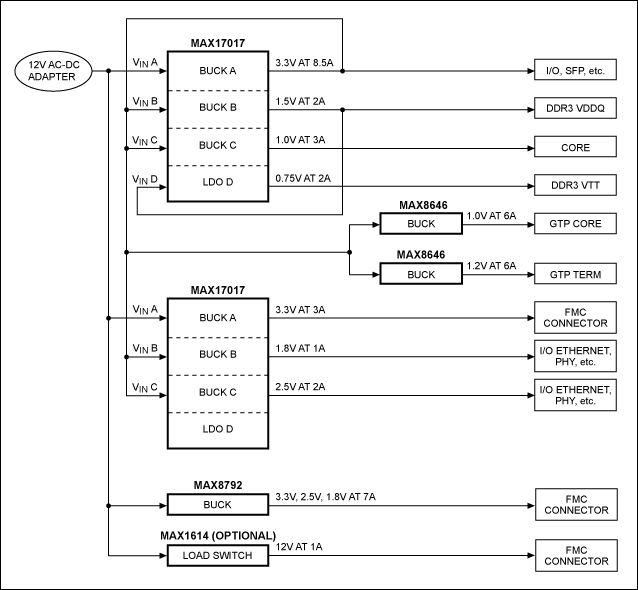
Figure 15. Block diagram of a Virtex-6 LX130T development platform, using Analog power supplies.
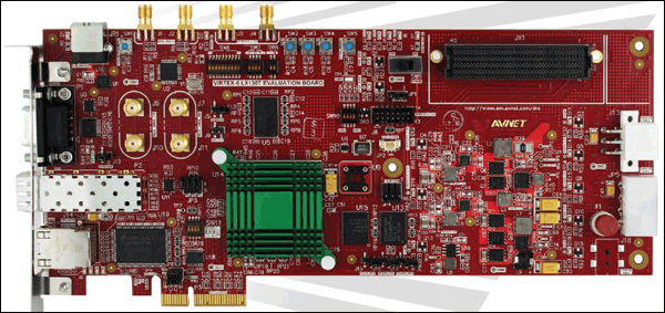
Figure 16. The Avnet Xilinx Virtex-6 LX130T evaluation kit employs the MAX17017.
Powering Spartan-6 FPGAs
Figure 17 shows a block diagram for a Spartan-6 LX150T FPGA power-supply design with built-in transceivers, where Analog PMIC regulators are powering all supply rails.
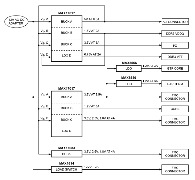
Figure 17. Block diagram of a Spartan-6 LX150T power-supply design that uses Analog power supplies.
Figure 18 shows a block diagram for a Spartan-6 LX16 FPGA power-supply design, where Analog PMIC regulators are powering the smallest Spartan-6 FPGA.
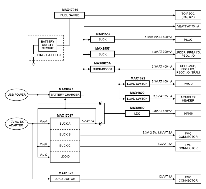
Figure 18. Block diagram of a Spartan-6 LX16 power-supply design, using Analog power supplies.
CoolRunner-II CPLD Power
CoolRunner-II CPLDs are often used in industrial and automotive applications that operate from a 24V nominal rail and need low quiescent current and light load efficiency. Figure 19 and Figure 20 show a CoolRunner-II CPLD board that is powered by Analog power regulators. This board also features Analog's 1-Wire secure EEPROM for IP security.
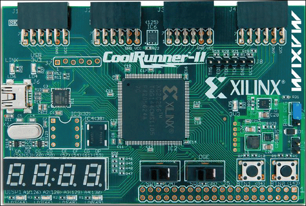
Figure 19. The CoolRunner-II CPLD board.
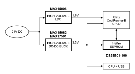
Figure 20. Block diagram of the CoolRunner-II CPLD board in Figure 20.
Summary
The first step in designing power supplies for FPGAs is to identify the system level requirements, such as the supply rail voltages and currents. FPGA power estimators assist in calculating these voltages and currents. From this, the designer should consider the advanced system level features, such as PMBus control, sequencing, and soft-start. Analog has several power-supply solutions to address the needs of FPGA application designers, from simple power regulators to advanced system-level power-management ICs with reference designs.
关联至此文章
产品
数字温度计和温度监控器
高端电源
三输出buck控制器,提供跟踪/排序功能
带有PMBus接口的数字电源控制器/监测器
1.425V至3.6V输入、2A、0.2V压差的LDO稳压器
1.425V至3.6V输入、2A、0.2V压差的LDO稳压器
1.425V至3.6V输入、1A、0.2V压差的LDO稳压器
4A、超低输入电压LDO稳压器
1.425V至3.6V输入、1A、0.2V压差的LDO稳压器
4A、超低输入电压LDO稳压器
低噪声500mA LDO稳压器,2mm x 2mm TDFN封装
1.425V至3.6V输入、1A、0.2V压差的LDO稳压器
1.425V至3.6V输入、2A、0.2V压差的LDO稳压器
结构紧凑的低成本1S/2S电量计
PMBus电源数据记录器
PMBus 6通道电源管理器
PMBus 5通道电源管理器和智能风扇控制器
高边、N通道MOSFET开关驱动器
高效、4A、1MHz、降压型调节器,内置开关,采用2mm x 2mm封装
低成本、3A、4.5V至28V输入、350kHz PWM降压型DC-DC调节器,内置开关
15A、降压型调节器,内置开关
高效、18A、电流模式同步整流降压调节器,内置开关
高效、8A、电流模式同步整流降压型开关稳压器
尺寸最小的1A、1.4MHz降压型稳压器
3A、2MHz、降压型调节器,内置开关
三输出buck控制器,提供跟踪/排序功能
4A、2MHz、降压型调节器,内置开关
可接受高输入电压的四输出控制器
1MHz、1%精度、6A内置开关、降压型调节器
16µA IQ、1.2A PWM降压型DC-DC转换器
尺寸最小的1A、1.4MHz降压型稳压器
高效、12A、电流模式同步整流降压转换器,内置开关
低电压、内置开关、降压型调节器
低压差、宽输入电压范围、降压型控制器
40V、高性能、同步buck控制器
高效、无缝切换升/降压型DC-DC转换器
2.2MHz、3A buck或boost转换器,集成高边开关
高效、2A、电流模式同步整流、降压型开关调节器
1MHz、全陶瓷、2.6V至5.5V输入、2A PWM降压型DC-DC稳压器
低压差、宽输入电压范围、降压型控制器
双输出buck控制器,提供跟踪/排序功能
低成本、小尺寸、能够工作在4.5V至28V宽电压范围的DC-DC同步buck控制器
双通道、可组合的QPWM图形核控制器,用于笔记本电脑
高效、4A、降压型DC-DC调节器,内置功率开关
1MHz、全陶瓷、2.6V至5.5V输入、2A PWM降压型DC-DC稳压器
低压差、宽输入电压范围、降压型控制器
单通道Quick-PWM降压型控制器,具有动态REFIN
6A、2MHz、降压型调节器,内置开关
双通道、4A/2A、4MHz、降压型DC-DC调节器,提供跟踪/排序功能
3A、1MHz、1%精度、内置开关的降压型调节器,带有电源就绪指示
双路、180°异相、1.4MHz、750mA、降压型调节器,带有POR和RSI/PFO
InTune自动补偿数字PoL控制器,带有驱动器和PMBus遥测
双路、5A、2MHz降压型调节器
高效、4A、1MHz、降压型调节器,内置开关,采用2mm x 2mm封装
6A、2MHz、降压型调节器,内置开关
4.5V至28V宽输入范围、双路输出同步buck控制器
单相/多相、降压型、DC-DC转换器,每相可提供高达25A的电流
双路、180°异相、1.4MHz、750mA、降压型调节器,带有POR和RSI/PFO
1.8A降压型调节器,提供远端检测,2mm x 2mm WLP封装
用于低功率架构的四输出控制器
40V、高性能、同步buck控制器
2.2MHz、3A buck或boost转换器,集成高边开关
双路、4A/2A、4MHz、降压型DC-DC调节器,提供双LDO控制器
双路、3A、2MHz降压型调节器
InTune自动补偿数字PoL控制器,带驱动器和PMBus远端检测
双路、180°异相、1.4MHz、750mA、降压型调节器,带有POR和RSI/PFO
高效率、10A、PWM降压型调节器,内置开关
12V、8A、1.2MHz、降压型调节器
24V、600mA内置开关、100%占空比、降压型转换器
资源
最新视频 21


