摘要
Four significant issues impact TD-SCDMA receivers: Phase noise, Noise figure, I/Q phase imbalance and power supply noise. Error vector magnitude is used to specify describe the influence of these factors on the radio receiver. Equations are given to estimate the impact of power supply noise, I/Q balance and LO phase noise.
Additional Information:
- Wireless Product Line Page
- Quick View Data Sheet for the MAX8877/MAX8878
- Applications Technical Support
Introduction
Time division, synchronous code division multiple access (TD-SCDMA) user equipment (UE) receiver design must balance the impact of many factors in meeting the system sensitivity specification. It is rudimentary to calculate the sensitivity using cascade noise figure techniques. The designer must also consider voltage controlled oscillator (VCO) phase noise, in-phase/quadrature (I/Q) phase balance, and power supply noise in calculating the receiver's sensitivity. This article presents the equations for including these issues by using error vector magnitude (EVM) calculations.
Some Factors Related to Sensitivity Specification
Reference sensitivity performance may be the most important specification for a receiver. Generally, it refers to the minimum input-power level at the antenna port while the system meets a needed bit-error-rate (BER). There are seven items that impact this specification:
- The noise figure of the receiver
- The transmitter's noise floor
- I/Q gain imbalance
- I/Q quadrature phase imbalance
- Phase noise
- Voltage noise of power supply
- Linear phase distortion
- Linear amplitude distortion
Item 1 and item 2 describe the influence of added white noise, so we can use the combined noise figure to describe these two items. With TD-SCDMA handset design, duplexing is time division duplex (TDD). With TDD operation, when the receiver is on, the transmitter should be turned off, so the noise floor of the transmitter is not an issue for TDD mode handset design.
Item 3, I/Q gain imbalance may have no influence for SNR specification, so if the baseband circuitry uses properly demodulates the signal, a 2 or 3dB difference between I and Q branch can be accommodated. Item 6, the noise of the power supply, can influence the signal path by two means:
- Most active circuits will act as amplitude modulators. This action is caused by the gain varying in response to the noise on their power supply lines.
- The VCO acts as a phase modulator. Usually this is not an issue for handset designing, for the voltage noise is usually very small, such as MAX8878, the spec is 30µVrms over 10Hz to 100KHz. Item 7 and Item 8 are linear distortion, and can be compensated by the baseband processor. Because the digital signal processor (DSP) can eliminate this type of distortion, we will neglect these two items in this article.
Below we will discuss the four issues most significant issues in UE receiver design: phase noise, noise figure, I/Q phase imbalance and power supply noise in detail. Error vector magnitude (EVM) will be used to quantify these items.
Error Vector Magnitude
EVM specification is often used to describe the modulation accuracy of the transmitted signal. TD-SCDMA and wideband CDMA (WCDMA) standards all use this specification to indicate the quality of the transmitted signal. We know that the receiver's BER specification is often described as the function of SNR (or Eb/No). Is there a relationship between EVM and Eb/No? 3GPP TS25.102 gives the EVM definition as below:
The error vector magnitude is a measure of the difference between the (ideal) waveform and the measured waveform. The difference is called the error vector. Both waveforms pass through a matched root raised cosine filter with bandwidth corresponding to the considered chip rate and the roll-off α = 0.22. Both waveforms are then further modified by selecting the frequency, absolute phase, absolute amplitude and chip clock timing so as to minimize the error vector. The EVM result is defined as the square root of the ratio of the mean error vector power to the mean reference power expressed as a %.
From the above definition, we know that Eb/No =1/ (EVM)². "Eb" is the energy per bit, "No" is the SSB noise power density per Hz. Now we will try to find the relationship between EVM and NF, phase noise, I/Q gain imbalance and I/Q phase imbalance. For simplifying calculation, we only consider QPSK modulation type and Es =2Eb for this type modulation, Es is the energy per transmitted symbol.
Noise Figure and EVM
Assuming the input signal power level is Ps, the cascade noise figure is NF, we have equations below:
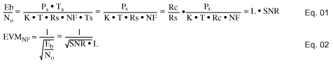
Note: Ts is the period of one transmitted symbol, T is the absolute temperature, assumed here to be 290°K, K is Boltzmann's constant, Rs is the symbol rate, Rc is the chip rate, L is the spreading factor (SF), and SNR is the signal-to-noise ratio.
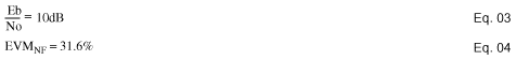
For TD-SCDMA handsets, the standard requires -108dBm reference sensitivity level, and suggests a 9dB noise figure. We will assume a 7dB noise figure, which allows a 2dB margin. "L", the spreading factor, is 16, and the chip rate is equal to 1.28Mbps (mega bits per second). Inserting these values to the above equations gives the following results:
Phase Noise and EVM
The diagram below can help understanding how the phase noise affects the signal quality:
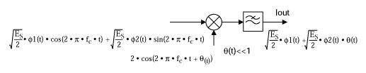
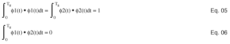
Note here Φ1(t) and Φ2(t) are two radices function, and they have below property:
Now project the Iout signal to Φ1(t) radix:
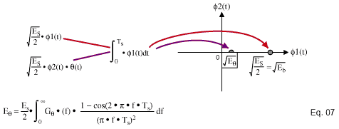
Note: GΘ(f) is the DSB phase noise power density.

Then:

Usually there is no problem with this specification. If we consider below a typical local oscillator (LO) phase noise specification, one can then calculate the EVMp spec.
| Offset (HZ) | 1 | 10 | 100 | 1K | 5K | 10K | 20K | 50K | 100K | 500K | 1M |
| dBc/Hz | -61 | -63 | -67 | -75 | -78 | -82 | -84 | -89 | -105 | -115 | -125 |
Consider the chip rate equal to 1.28Mbps (for the TD-SCDMA standard), L equal to 16. These results are obtained:
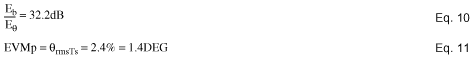
This is a very good result. It shows no significant degradation of the signal. According to TD-SCDMA standard, the above LO phase noise specification causes no problem for the reference sensitivity specification. The reference sensitivity is the minimum receiver input power measured at the antenna port at which the BER does not exceed a specified value. The BER shall not exceed 0.001 for the parameters specified in Table 1.
| Parameter | Level | Unit |
| ΣDPCHo_Ec / Ior | 0 | dB |
 |
-108 | dBm/1.28MHz |
From the above standard requirement, all the input power is signal, with no other code channels. In the case of a practical working environment, the handset will receive many other code channels. In the ideal case, the other codes will be no problem since all the signals are orthogonal. When one considers the phase noise influence, and calculates the EΘ with eqn. 7, it is found to be a serious problem. The table below gives the dedicated channel (DCH) parameters in multipath case 1 channel:
| Parameters | Unit | Test 1 | Test 2 | Test 3 | Test 4 |
| Number of DPCH0 | 8 | 2 | 2 | 0 | |
| ΣDPCHo_Ec / Ior | dB | -10 | -10 | -10 | 0 |
| Ioc | dBm/1.28MHz | 60 |
|||
| Information Data Rate | Kbps | 12.2 | 64 | 144 | 384 |
DPCH : Dedicated physical channel
IOR : CDMA power spectral density of forward channel
IOC : power spectral density of interfering noises and signals
EC : power spectral density of a single channel
In Test 1, you will find that Ec/Ior is -19dB, so EΘ will be increased 19dB, giving the result below:
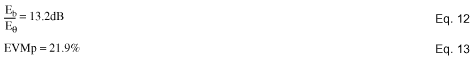
Compared with equations 3 and 4, this is not adequate performance. Good design practice dictates a 3dB margin to account for multipath fading. To accomplish this, the phase noise specification should be improved by 3dB at 1KHz, 10KHz, 20KHz offset. ΘrmsTs should be less than 1.1°.
Power Supply Noise
The noise of the power supply can affect the LO's phase noise. Show below is a simple equation to estimate the influence of the power supply noise:
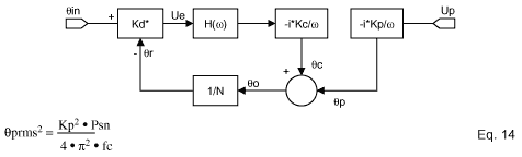
Kp is the pushing coefficient of VCO, Psn is the noise power of the power supply, fc is the 3dB corner frequency of the PLL filter.
For example, the Kp specification of MAX2392's VCO is 2MHz/V, Psn specification of MAX8878 is 900µVrms² over 10Hz to 100KHz. Assuming a PLL bandwidth of fc equal to 5KHz, and we get the following result:
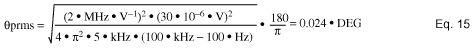
This RMS phase noise is acceptable, mainly due to the low noise of the MAX8878.
Demodulator Phase Imbalance
Any I/Q demodulator will possess a phase error due to a mismatching in the two paths. This phase error will have the effect of attenuating the signal power, thereby reducing the signal to noise ratio. The I/Q phase imbalance only impacts the reference sensitivity, and usually it is very small. Below is an equation to calculate the degradation in sensitivity due to the phase error:
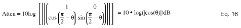
If Θ=5°, the SNR is attenuated by 0.017dB. This amount of SNR decrease is negligible.
{{modalTitle}}
{{modalDescription}}
{{dropdownTitle}}
- {{defaultSelectedText}} {{#each projectNames}}
- {{name}} {{/each}} {{#if newProjectText}}
-
 {{newProjectText}}
{{/if}}
{{newProjectText}}
{{/if}}
{{newProjectTitle}}
{{projectNameErrorText}}
最新视频 21


