No Latency Delta-Sigma ADC Techniques for Optimized Performance
Introduction
Linear Technology’s Delta-Sigma analog-to-digital converter product family simplifies a variety of applications. The products’ ease-of-use and high accuracy without the need for calibration, external clocks or complex interfaces enables designers to rethink their system architectures.
Although 24 bits may seem excessive to some, many designers find significant advantages with these higher resolution converters. One such advantage is the elimination of front-end amplification. This enables direct digitization of many sensors while removing problems associated with front-end offset and gain errors as well as simplifying tare adjustments. One misconception commonly solved by designers using the LTC2400 family is the relationship between speed and resolution. Many designers have found that higher speed ADCs with averaging do not meet the one-shot performance of the LTC2400 family. The absolute accuracy of the LTC2400 family is demonstrated using a bridge sensor in a weigh scale application.
Product Family Overview
The LTC2400 product family (see product family tree in Figure 1) is divided into single-ended and differential input devices. The single-ended devices have pin-compatible 20-bit and 24-bit versions with 1-, 2-, 4- and 8-channel implementations. The differential parts offer ultralow noise (as low as 800nVRMS) tiny packages (as small as MSOP-10) and simultaneous 50Hz/60Hz rejection (LTC2413). Future products include multichannel, 20-bit, pin-compatible differential devices and high speed devices.

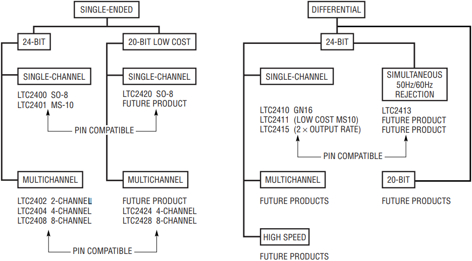
Figure 1. The LTC2400 product family.
Several key features common to the LTC2400 family differentiate it from other high resolution converters currently available. The first feature is a highly accurate on-chip oscillator enabling 110dB minimum rejection of AC line frequency interference with no external frequency setting devices required. The second feature is the absence of digital filter settling delay. This enables simple multiplexing without the need to sift through redundant or useless data. The LTC2400 family offers continuous offset and full-scale calibration that is transparent to the user. This results in an offset accuracy of less than one part-per-million (ppm) with 0.002ppm/°C drift and full-scale accuracy of less then 4ppm with drifts less than 0.01ppm/°C. The overall (absolute) accuracy (offset + full-scale + linearity + temperature drift) is typically within ±2ppm total error (see Figure 2).


Figure 2. Absolute accuracy: total unadjusted error vs temperature.
Based on these exemplary performance characteristics, the LTC2400 family of converters can be used in several unconventional ways, resulting in simpler designs with improved system performance.
Eliminating Front-End Amplification (No PGAs)
Programmable gain amplifiers (PGAs) are typically used in front of analog-to-digital converters to amplify low level input signals in order to improve the overall noise performance. Simply put, a PGA increases the input signal seen by the ADC, thereby reducing the effective LSB step size at the input while reducing the input span.
Generally, designers apply enough gain in the analog front end to use the full dynamic range of the ADC. For example, if a sensor produces a signal between 0mV and 20mV (see Figure 3), a front-end amplification of 250× increases the signal applied to the ADC to 5V. This corresponds to 16,384 counts from a 14-bit ADC. The same 20mV sensor signal applied directly to the LTC2410 (22.6 effective bits) yields 25,000 counts. Rather than use the whole dynamic input range of a low resolution ADC (12, 14 or 16 bits), the sensor input is applied to a fraction of the input range of a high resolution ADC (20 or 24 bits). Direct digitization has several advantages over designs using front-end amplification.

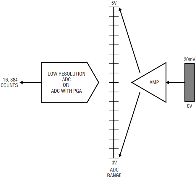
Figure 3a. 14 bits + gain of 250.

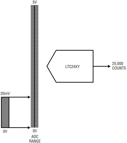
Figure 3b. 24 bits + no gain.
Direct Digitization Eliminates PGA Offset Errors and Handles Sensor Tare Easily
One problem associated with front-end amplification is the effects of offset errors and tare adjusts. For example, a small offset applied to the front-end amplifier causes the ADC input to exceed the dynamic input range (see Figure 4). These offset/tare values must be removed from the sensor signal prior to amplification. This results in added complexity in the analog input path. On the other hand, since the LTC2410 only uses a small percentage of its dynamic input range, even large offsets/tare voltages can simply be removed digitally. Furthermore, the offset (<1ppm) and drift (0.002ppm/°C) of the LTC2410 are negligible when compared to those associated with a front-end amplifier and a low resolution ADC.

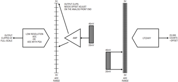
Figure 4. Offset and tare adjustments are difficult to remove with front-end gains, but are easy with the LTC24XY family.
Direct Digitization Eliminates PGA Gain Errors
A second problem associated with PGAs and overcome by direct digitization using the LTC2400 family is gain and gain drift. In order to implement a PGA, external ratioed resistors are commonly used. Mismatch between these resistors and variations with temperature lead to system-gain errors. ADCs with built in PGAs use capacitor ratios to set the gain. Again, these ratios vary, leading to gain errors typically in the 0.1% range (10 bits). Direct digitization using the LTC2400 family eliminates these gain errors. For example, the total error associated with the LTC2410 is within ±1.5ppm (0.00015%) including temperature drift (see Figure 2). Therefore, direct digitization using the LTC2400 family offers significant performance advantages over conventional ADC/PGA designs while greatly simplifying the analog front end.
Speed Myths—Faster May Not be Faster
In the realm of high resolution ADCs, conversion rate is often misunderstood. One requirement designers often have for high precision DC measurements is AC line frequency rejection. The fastest rate at which a sinc4 ADC can produce fully settled data is at fNOTCH/4. In order for the LTC2415 to reject 60Hz, its output rate is 15Hz. Conventional delta-sigma converters output data faster, at fNOTCH (60Hz), but the higher speed is not as useful as it first appears because of redundant data. Each conversion result is a weighted average of the previous four conversion results. Despite the fact that conventional converters produce an output at a rate four times faster than the LTC2415, the useful conversion rate is the same.
More Readings ≠ More Useful Data
When comparing LTC2400 devices’ output rates to those of conventional delta-sigma ADCs, the issue of data latency must be considered. The LTC2400 filter has no latency: each conversion result is valid. Conventional delta-sigma converters produce the valid conversion result as well as redundant data. If the filter settling time is four cycles (4th order sinc filter), then three out of every four conversion results are redundant. Whenever the input changes (for example when a multiplexer input changes), the following three conversion results are inaccurate due to filter settling error.
As shown in Figure 5, a staircase input signal applied to a conventional delta-sigma converter (output data rate 60Hz) offers no advantage over the LTC2415 outputting data at 15Hz. Both devices offer 60Hz AC line frequency rejection and provide valid conversion results at a 15Hz rate. The only difference is the LTC2415 is not outputting the erroneous data associated with filter settling.

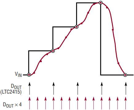
Figure 5. More readings ≠ more useful data.
Similarly, more readings/second does not yield higher input bandwidth (see Figure 6). In this case, an input signal changing synchronously with the output rate is not accurately captured due to the filter settling error. Each result is a weighted average of the previous four conversion results. In order for the conversion result to be valid, the input signal must be stable for four consecutive conversion cycles. Therefore, the higher output rate device offers no advantage in input signal bandwidth when compared to the LTC2415.

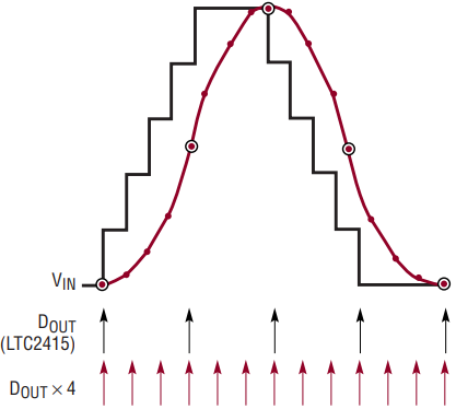
Figure 6. More readings per second ≠ higher input bandwidth.
More Readings + Average ≠ Better Noise Rejection
Delta-sigma converters consist of an analog modulator and a digital filter. One characteristic of the digital filter is high rejection at its notch frequencies, which are related to the output rate. In a conventional delta-sigma ADC, a 60Hz output rate yields excellent rejection (Sinc4) at 60Hz plus harmonics (see Figure 7).

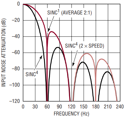
Figure 7. More readings + average ≠ better noise rejection.
If the output rate is doubled, the 4th order filter notch moves from 60Hz to 120Hz. If this doubled output rate data is averaged 2 to 1, the effective output rate becomes 60Hz. The 4th order null remains at 120Hz and a first order (Sinc1) notch is created at 60Hz due to the 2:1 averaging. The notch at 60Hz offers much less rejection than the same device operating at a 60Hz output (Sinc4 notch at 60Hz) as well as lower overall noise rejection when compared to the ADC operating at the lower speed. Increasing the data output and averaging does not improve the noise rejection.
More Readings + Average ≠ Higher Resolution
Many conventional delta-sigma converters offer higher output rates at the expense of decreased resolution. Many system designers, in an effort to increase the overall system resolution, run these converters at the fastest rate and then average the results. As previously seen, this does not improve the noise rejection of the ADC.
The analog portion of a delta-sigma ADC consists of a high order modulator sampling the input signal many times faster than the actual output rate; this ratio is defined as the over-sample ratio (OSR). In the case of a 3rd order modulator, for every doubling in OSR, the noise improves 3.5 bits. One way to increase the output rate is to decrease the OSR. As shown in Figure 8, every time the output rate is doubled (OSR is reduced by 2), the resolution decreases by 3.5 bits. Every time the number of averages is doubled, the resolution only improves by 0.5 bits. As shown in Figure 8, by starting with a 24-bit device and decreasing the OSR by 8× (speeding up the device by 8×), the resolution decreases to 14.5 bits. Once the eight samples are averaged to a normalized output rate of 1, the resolution improves by 1.5 bits, to 14 bits, 10 bits worse than the initial part running at the original output rate.

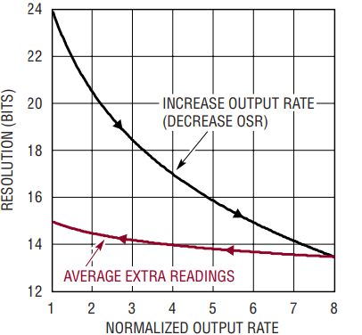
Figure 8. More readings + average ≠ higher resolution.
As an example, a commonly used, conventional, high resolution delta-sigma ADC offers a fast mode, 64kHz output rate with a resolution of 11 bits. This is 853 times faster than the LTC2410 operating at 7.5Hz output rate with a resolution of 22.6 bits. By averaging the extra 853 conversion results, the 11-bit resolution is improved by 0.5 • log(853)/log(2) ≈ 5 bits, resulting in 16 bits overall resolution. This result does not take into account the redundant data. The 64kHz output rate contains three out of four redundant output data due to filter settling. This results in a √2 penalty in averaging, or loss of 0.5 bits resolution. This leaves only 15.5 bits resolution with the overhead of averaging 853 data points, compared to the 22.6-bit single-shot resolution of the LTC2410.
Demonstration—Direct Digitization
In order to demonstrate the ease of use and accuracy of the LTC2400 family, a 10mV full-scale bridge is mounted to a weigh scale and directly digitized by the LTC2410 (see Figure 9). Measurements are taken using demonstration board DC291A (available to qualified customers—contact LTC Marketing for information). Various measurements were taken and the output of the demonstration program screen was captured and presented here.

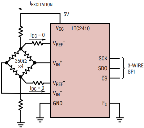
Figure 9. Direct digitization with the LTC2410.
The first two measurements (see Figure 10) are the result of the an empty scale (digital tare established) and the scale with a nickel (U.S. 5 cent coin) applied. Initially, the ADC measures 36.0674ppm of full-scale (corresponding to a sensor tare of 180µV). With the coin applied, the ADC reads 36.274ppm of full-scale. Digitally removing the tare voltage, the weight of the nickel corresponds to 0.21ppm or 1.05µV.

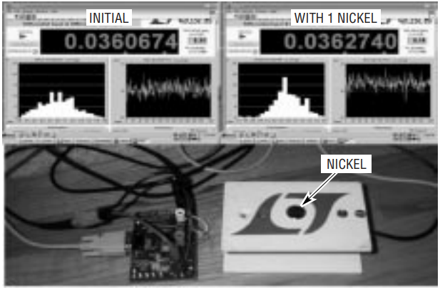
Figure 10. Measurement results: initial (left) and with one nickel (right).
Next, the nickel is removed from the scale and a bag of 15,000 pennies (U.S. 1 cent coin) is applied to the scale, see Figure 11. The ADC output reads 1110.3683ppm or 1/1000 of the full-scale output of the ADC and one-half of the full-scale output of the sensor. The nickel is then added on top of the 15,000 pennies (see Figure 12). The ADC reads 1.1106087ppm of full-scale. Subtracting the measurement of the bag of pennies from the bag of pennies plus the nickel yields 0.24ppm of full-scale. This result is within 0.03ppm (0.000003%) of the initial measurement of the nickel alone, exemplifying the absolute accuracy of the LTC2410 and the advantage of direct digitization.

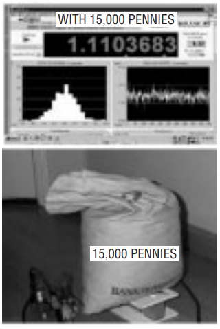
Figure 11. Measurement results with 15,000 pennies.

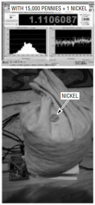
Figure 12. Measurement results with 15,000 pennies and one nickel.
Conclusion
Over the past several years, Linear has introduced a family of twelve delta-sigma analog-to-digital converters based on a revolutionary new architecture, enabling ease of use and high accuracy. The accuracy of these devices enables many applications currently using PGAs to migrate to direct digitization. The advantages of direct digitization include simple sensor offset/tare handling, no PGA gain error problems, and reduced cost/increased simplicity by removing analog front-end circuitry. Additionally, its high order on-chip filter and 2ppm one-shot accuracy yields better performance than comparable parts running at much higher output rates. Linear has many demonstration boards and simple software available to qualified customers for quick evaluation of the LTC2400 family.
关于作者
关联至此文章
{{modalTitle}}
{{modalDescription}}
{{dropdownTitle}}
- {{defaultSelectedText}} {{#each projectNames}}
- {{name}} {{/each}} {{#if newProjectText}}
-
 {{newProjectText}}
{{/if}}
{{newProjectText}}
{{/if}}
{{newProjectTitle}}
{{projectNameErrorText}}
最新视频 21


