摘要
In this application note a circuit with two switched-capacitor filters reconstructs the output of a digital-to-analog converter (DAC) while providing anti-aliasing and sinc-compensation functions. Filter IC prevents alias frequencies by excluding spectral energy above fs/2. The MAX265 filter is featured.
The dual-biquad filter chips and some external components (Figure 1) form a multipurpose filter for the reconstruction of D/A converter signals. Connected to a converter's output (Figure 2), the filter aids in generating the analog signal represented by digital-data samples at the converter's input. In addition, the filter provides anti-aliasing, (sinπx)/πx (sinc) compensation, and reduction of the D/A converter's quantization noise.

Figure 1. Configured as shown, two filter ICs reconstruct the output of D/A converter while providing antialiasing and sinc-compensation functions.
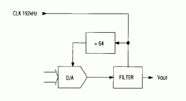
Figure 2. In a suggested application for the Figure 1 circuit, the applied clock signal and single-chip divider set the desired sample rate for the D/A converter.
At, DC, a D/A converter's output is easily predicted from it's data sheet specs. Time-varying signals, however, produce staircase-output waveforms whose reconstruction errors are best discussed in the frequency domain. The converter's output spectrum, for example, consists of spectra (±f1, where f1 is the spectrum represented by the digital input samples) that repeat at integral multiples of the sample rate fS (Figure 3).
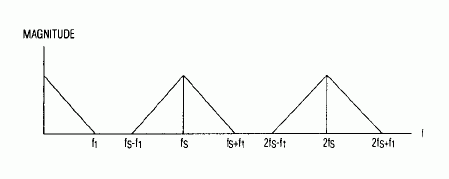
Figure 3. Figure 2's digital-input spectrum F1 combines with the D/A converter's sampling rate fS as shown, producing a ±f1 spectrum that repeats at integral multiples of fS.
The filter's first job is to prevent alias frequencies by excluding spectral energy above fS/2. In practice, f1 < fS/2. The filter should pass f1 with an acceptably low error while sufficiently attenuating all frequencies above fS/2.
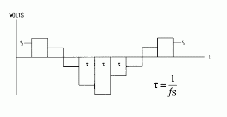
Figure 4. Before filtering, the D/A converter's output signal is a staircase waveform that can be regarded as a sequense of rectangular pulses.
A second filter requirement stems from the presence of sinc attenuation, introduced by the effect of rectangular-pulse components in the staircase waveform (Figure 4). These pulses have the same 1/fS width, but differ in amplitude according to the digital-sample magnitudes. The spectrum of each pulse is the Fourier transform (the sinc function of f/fS). These spectra combine with the f1 spectrum to form an overall frequency response for the converter output. Note the sinc expression's variation in amplitude for various values of f:
| f | [(sin)(πf/fS]/(πf/fS) |
| 0 | 1.0 |
| fS/4 | 0.9003 (-0.9dB) |
| fS/3 | 0.8270 (-1.65dB) |
| fS/2 | 0.6366 (-3.92dB) |
Clearly, the staircase approximation causes an increase amplitude error as f approaches the Nyquist frequency fS/2. To compensate for this attenuation, the Figure 1 circuit incorporates the inverse expression (πf/fS)/sin(πf/fS) in it's passband-magnitude response.
Ideally, the resulting filter response would provide sinc compensation to fS/2, drop abruptly to zero, and maintain that infinite attenuation for all frequencies above fS/2. But actual filters cannot provide abrupt transitions or infinite attenuation. As a practical compromise, the circuit makes its transition over a finite bandwidth (transition ratio), and then provides an out-of-band rejection comparable to the D/A converter's signal-to-noise ratio SNR.
SNR for an ideal D/A converter is about 6dB/bit, or 72dB for a 12-bit device. Quantization error further degrades this number, yielding about 68dB for a typical 12-bit converter. Thus a reasonable goal in Figure 1 is 70dB rejection above fS/2.
To prevent aliasing, the stopband edge must be no greater than the Nyquist frequency (fS/2). The passband edge must threrfore be less than fS/2. To achieve 70dB stopband rejection in the 8th-order circuit of Figure 1, the required transition ratio (fStopband/fPassband)) is 1.5, which sets the passband edge at fS/3. A rising amplitude response within this passband compensates for the converter's sinc attenuation.
Perfect sinc compensation would provide 1.65dB of gain at the Nyquist frequency, but tolerance uncertainties in the ±1% resistors and within the filter ICs limits the actual correction to about 1dB. The circuit does, however, achieve the 70dB stopband rejection and the 1.5 transition ratio. Figure 5 compares the Figure 1 response with that of an ideal filter.
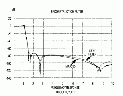
Figure 5. The circuit response of Figure 1 compares well with that of an ideal filter.
To assure maximum dynamic range, the four biquad-filter sections (two in each IC) exhibit increasing Q from input to output, The pole-zero pairs of each section also axhibit increasing frequency, which minimizes the spread in component values. The following pole and zero values produce a 1-rad/sec filter passband:
| Section | fpole (Hz) | Qpole | fZero(Hz) |
| 1 | 0.1005 | 0.5603 | 0.2397 |
| 2 | 0.1310 | 1.0540 | 0.2777 |
| 3 | 0.1564 | 2.3876 | 0.4273 |
| 4 | 0.1685 | 8.5145 | 1.4016 |
Note the feedback capacitors C1-C4 across each output op amp. These capacitors have two purposes; they improve the quality of transmission zeroes, and the form 1-pole lowpass filters that help to smooth out the discrete-level steps introduced by the filter's switched-capacitor action. The 1-pole filters have little effect on the passband shape because their high corner frequencies introduce only 0.1dB of loss at 1kHz.
Note also, that the applied clock frequency in Figure 2 (192kHz) allows use of a convenient binary-64 divider for setting the necessary 3X ratio betweeen the converter's sample rate and the filter's 1kHz corner frequency, f0. Each chip is programmed for an fCLK/f0 ratio of 191.64 by V+ and V- connections to the filter inputs, F0-F5.
关联至此文章
产品
最新视频 21


