Managing Noise in the Signal Chain, Part 2: Noise and Distortion in Data Converters
Read other articles in this series.
摘要
Data converters incorporate the common semiconductor noise sources such as, shot, avalanche, flicker, and popcorn noise. In addition, real data converter systems have errors that include quantization, clock jitter, channel linearity, and bandwidth. Practical use of industry data sheets demonstrated to determine what system specifications can be achieved. Design tools that aid in the analysis of these parameters, and constructive ways to control and reduce other system noise elements will be presented.
A similar version of this article appears on EDN, November 2, 2013.
Introduction
This is the second in a three-part series on noise in the signal chain. In Part 1 we identified the origins and characteristics of noise found in all semiconductor devices and explained how it is specified in device data sheets. We showed how to estimate the output noise of a voltage reference under real-world conditions that are not specified in the data sheet. In this article we focus on the sources of noise and distortion particular to ADCs and DACs. As before, we show how this noise is specified in a data sheet. Part 3 of the series will bring Parts 1 and 2 together, and show readers how to optimize their noise budget and choose the most appropriate data converter for their application.
Noise In the Signal Chain
The sources of noise in a signal chain can be either internal or external. Managing noise in the signal chain requires meticulous examination of each circuit in the chain to minimize noise where possible. This is elementary and pivotal to our discussion because noise, once embedded in a signal, is very difficult or impossible to remove.
It is important that we start by briefly reviewing a few basic, but critically important, topics from the Part 1 article on Annoying Semiconductor Noise. Understanding electrical noise is more essential today than it has ever been. As 14- and 16-bit data converters become mainstream and 18- and 24-bit converters are increasingly available, noise is often the single factor that limits a system’s performance. There is no doubt that recognizing its origins and characteristics is key to achieving a signal chain’s greatest possible accuracy.
Generally speaking, noise is any electrical phenomenon that is unwelcomed in an electrical system. Depending on its origin, noise can be classified as external (interference) or internal (inherent). This article will focus on the noise inherent in all data converters and caused by the sampling process.
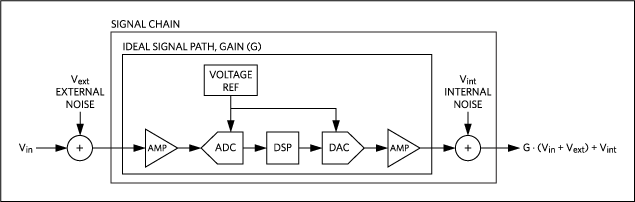
Figure 1. Noise in the signal chain.
In Figure 1 all external noise sources are combined into the term Vext. All internal noise sources are combined into the term Vint.
Now we will examine the four common types of noise and distortion in data converters: quantization noise, sample jitter, harmonic distortion, and analog noise.
Noise in Data Converters
Quantization Noise
Quantization noise is the most well-known source of noise in a data converter. It results from the errors inherent in the sampling and quantization process used in the converter. The magnitude of this noise is determined by three factors: resolution, differential nonlinearity, and bandwidth.
Resolution
Quantization is the uncertainty that results from dividing a continuous signal into 2N discrete levels, where N is the resolution in bits. All analog voltages within a given quantum have the same code, which results in a quantization uncertainty. This uncertainty is called the “quantization error.” The root mean square (RMS) value of the quantization error is the quantization noise. Quantization error is inversely proportional to 2N. The quantization error over time for an ideal ADC is shown in Figure 2, which also shows how quantization error reduces as the resolution increases.
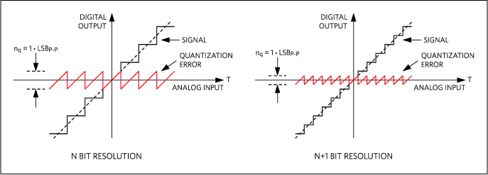
Figure 2. Quantization error results from dividing a continuous signal into 2N discrete levels.
The RMS quantization noise of an ideal data converter of resolution N is given by:
nq = 20 × log(1/(√12 × 2N))
Or in terms of LSB:
nq = 1/√12 LSBRMS
Differential Nonlinearity
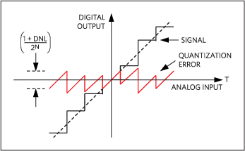
The differential nonlinearity (DNL) of a data converter is the deviation of any code width from an ideal 1 LSB step. An ideal data converter would have a DNL of 0, but most precision data converters today have a DNL < 1. The average DNL of a data converter increases its average quantization error and, therefore, its quantization noise (Figure 3).
 0.">
0.">
Figure 3. Quantization error over time, DNL > 0.
The average DNL is usually not specified in a data converter data sheet, however, the typical DNL specification can be used in its place with reasonable accuracy.
The RMS quantization noise, including the effects of resolution (N) and DNL, is given by:

Or in terms of LSB:

Bandwidth
The quantization noise described to this point has assumed the use of the full Nyquist bandwidth.
If the sample frequency (Fs) and the input signal are harmonically uncorrelated, then the quantization noise is Gaussian and distributed evenly between DC and the Nyquist frequency (Fn). The Nyquist frequency (Fn) is always half the sample frequency (Fs). This noise spectral density is shown in Figure 4.
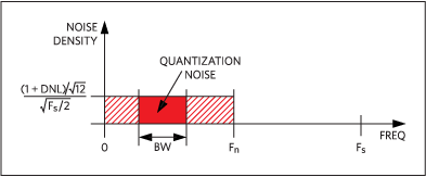
Figure 4. Quantization noise spectral density over bandwidth.
In Figure 4 the quantization noise voltage is the noise under the noise density curve within the operating BW.
The RMS quantization noise, including the effects of resolution (N), DNL, and BW is given by:

Or in terms of LSB:

Where BW is defined as a percentage of the Nyquist frequency (Fn).
Finally, Equations 5 and 6 indicate that quantization noise can be decreased by increasing resolution (N), decreasing average DNL, and decreasing BW.
This model assumes that all out-of-band noise has been removed by filtering, i.e., using an ideal brick wall filter in the out-of-band regions. The model also assumes that no noise shaping is used. In practice, not all out-of-band noise can be removed, so the actual noise will be somewhat higher than predicted.
Oversample Rate
Alternatively, the oversample ratio (OSR) can be used in place of BW. OSR is the ratio of a higher sample rate OSR·Fs to the original sample rate Fs. OSR assumes that the original BW remains unchanged, 0 to Fn, where Fn = Fs/2.
As defined, BW and OSR are related by:
OSR = 100%/BW
The noise density spectrum for an oversampled data converter is shown in Figure 5.
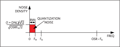
Figure 5. Quantization noise spectral density with OSR.
The RMS quantization noise, including the effects of resolution (N), DNL, and OSR is given by:

There will be a 3dB deduction in noise per octave of oversampling. The noise in LSBRMS is given by:

Sample Jitter
Sample jitter (tj) is a source of noise found in all sampled systems, including data converters. It can be caused by internal and external sources. Internally, an ADC’s sample-and-hold circuit can introduce aperture jitter that contributes to sample jitter. Externally, phase jitter in an external sample clock can add noise to both ADCs and DACs.
Sample jitter introduces noise when sampling a time-varying signal. It produces unwanted variations in sampled values, as shown in Figure 6.
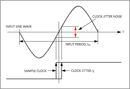
Figure 6. Sample jitter noise.

Or in terms of LSB:

Harmonic Distortion
Harmonic distortion of a signal is caused by the presence of unwanted harmonics. Nonlinearities within a channel are a common cause of harmonic distortion, as illustrated in Figure 7.
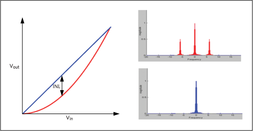
Figure 7. Harmonic distortion.
In data converters, nonlinearity is specified by integral nonlinearity (INL). INL is defined as the maximum deviation of the output from the ideal transfer function after gain and offset errors have been removed. Harmonic distortion, as one might imagine, is correlated with INL. As INL increases, the harmonic distortion increases. However, any influence that INL may have on total harmonic distortion (THD) is impossible to predict, because harmonic distortion depends on the shape of the transfer function and not just its maximum deviation from ideal.
THD is the standard measure of harmonic distortion and is defined as the ratio of the RMS sum of the first five harmonics to the full-scale RMS signal amplitude (Vfs).

The total noise contributed by harmonic distortion is the root-sum-square (RSS) of all harmonic components:

THD is not specified as an absolute noise level, but as a fraction of the full-scale RMS level. It is specified in either percentage or decibels. However, the resulting LSBRMS noise level can be found using the following equations. When THD is given in %, then:

When THD is given in LSB, then:

Output Buffer Distortion
Many output buffers are touted as rail-to-rail outputs. The buffers are really just op amps; as their outputs approach the power and ground rails (unipolar usage), they start running out of current. Many times output buffers are specified without any load, and in this condition they can get to within 20mV to 30mV of power and ground. However, when they are asked to supply even a few milliamps, they can only get to within 200mV to 300mV of the power and ground rails. Read the data sheet carefully. The data sheet may state that, “the output will get within 20mV of ground” (the real number), but other product literature might say that the output goes to zero volts—true only if the number is rounded to an integer.
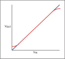
Figure 8. The transfer function, illustrating clipping and compression on the output.
Figure 8 exhibits the result of the output-driver current limiting near the power and ground rails. The blue line is linear and the red dotted line is nonlinear. As the signal voltage approaches the rail, current is reduced until the transistor can no longer function. The op amp requires current to close the feedback loop and linearize itself. We see that the input is changing on the left and right ends, but the output cannot respond at the top and bottom of the graph. This distortion in the transfer function of the output buffer will introduce harmonic distortion.
Analog Noise
Analog noise (Vn) is the effective noise referred to the input of an ADC or the output of a DAC. It is caused by the semiconductor noise sources discussed in Part 1 of this article series. It may be specified as noise spectral density in units of nV/√Hz, voltage in RMS or peak-to-peak, or LSB in RMS or peak-to-peak. Vn can originate from internal or external sources, is random, and is assumed to be Gaussian.
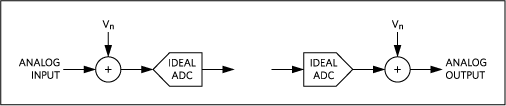
Figure 9. Analog input and analog output referred noise, Vn.
Vn is often given in units of LSBRMS. In ADCs Vn is called transition noise because it presents itself as an uncertainty at the time of transition from one output code to the next. When Vn is given in LSBRMS, the equivalent peak-to-peak noise can be found by:
nan = 6.6 × Vn LSBP-P
There are five common, fundamental sources of noise (Vn) found in semiconductors: thermal, shot, avalanche, flicker, and popcorn noise. These sources of noise are discussed in detail in Part 1 of this series, but now an additional noise source deserves mention: kT/C noise.
kT/C Noise
kT/C noise is found in all sampled-data systems and, along with quantization noise, places a fundamental limit on the performance of any ADC. kT/C noise is not a fundamental noise source. Rather, it is thermal noise in the presence of a filter capacitor, and is found in all sample-and-hold circuits at the input to ADCs.
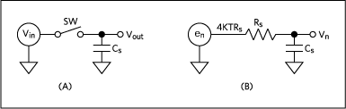
Figure 10. A simplified sample-and-hold circuit (A) and noise-equivalent circuit (B).
Figure 10(A) shows a simplified sample-and-hold circuit found at the input of ADCs. When the switch is closed the input voltage source (Vin) charges the sampling capacitor (Cs) to voltage at Vin. Figure 10(B) shows the noise-equivalent circuit. In this latter configuration, the switch is replaced by Rs which is the combined on-resistance of the switch and output impedance of the voltage source; Vin is replaced by the noise spectral density (en); and Vout is replaced by the output noise voltage (Vn). When the switch is closed, Cs is charged to the input voltage (Vin) plus the noise voltage (Vn).
The total output noise voltage (Vn) results from the thermal noise of Rs after being lowpass filtered by Cs. Any change in thermal noise due to a change of Rs is offset by an equal and opposite change in noise BW of the RC filter. As a result, Rs drops out of the noise equation (Equation 17) and has no effect on the total output noise. The output noise, which then is only a function of temperature and the sampling capacitor, is given by:
Vn = √(kT/CS) VRMS
Where k is Boltzmann’s constant and T is the temperature in Kelvin.
As a point of reference, a 1pF sampling capacitor leads to 64.4µVRMS of noise at room temperature. As the capacitance increases by a factor of x, the noise decreases by a factor of x½.
External Noise
We already discussed sources of internal noise, but there are also many sources of external noise. External noise can come from anywhere outside the signal chain itself, for example, from the power supplies, digital switching, radio frequency (RFI), and electromagnetic interference (EMI). Each of these external sources needs to be controlled by proper PC board (PCB) layout including grounds and ground star points. Power decoupling capacitors, lowpass filters, shielding for RFI and EMI all require a good understanding of the components and system. Capacitors and their self-resonance, series components such as inductors, ferrite beads and resistors all play important roles in minimizing intrusive noise.
How Noise Is Specified in Data-Converter Data Sheets
The following specifications have been taken from the MAX1062 ADC data sheet. This table shows how resolution, DNL, aperture jitter, THD, and analog noise will likely appear in a typical data sheet.
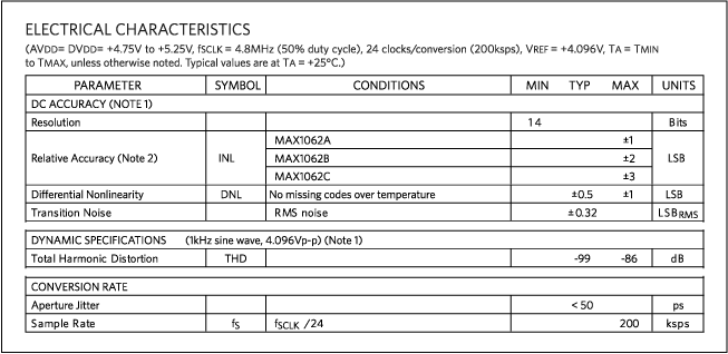
Figure 11. Noise-related portion of the EC table from the MAX1062 ADC data sheet.
The following table is taken from the MAX5170 DAC data sheet. It is another example of how noise may appear in a data sheet.
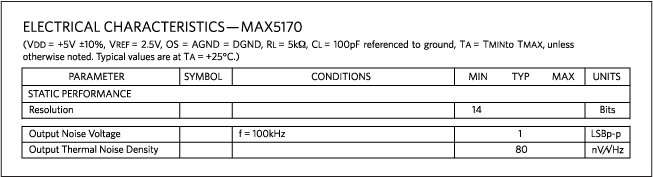
Figure 12. MAX5170 DAC data sheet.
Conclusion
In this article we learned how various data-converter parameters contribute to noise in the signal chain. These include resolution, differential nonlinearity, operating bandwidth, clock jitter, harmonic distortion, and input or output referred noise.
In Part 3 of this series, we will synthesize what we have learned about these data converter parameters. We will demonstrate how to use the EC table parameters to estimate their contribution to the total signal-chain noise and how to select the best data converter for a given noise budget. A free design tool will be introduced to help identify noise sources and improve signal-chain performance.
关联至此文章
产品分类
最新视频 21


