Make Your Automotive Dual USB Type-C with USB Power Delivery Design Cool and Flexible
摘要
This design solution reviews the challenges of designing an automotive dual USB Type-C™ with USB power delivery system. The module temperature rise must be below 40°C. The automotive battery voltage undergoes wide swings. The data lines must be adequately protected, and the design must be flexible and adaptable to different form factors. A buck-boost controller IC and a protection IC chipset enable a small and flexible module that operates within allowed thermal limits.
Introduction
USB ports are pervasive in automobiles. With the use of the proper cable, a number of portable devices, smartphones, and tablet PCs can be charged on the go. The electronic modules that implement these functions must fit inside small spaces without overheating. The problem is exacerbated in the case of dual-port dedicated charging solutions (Figure 1), which must support two connectors without increasing component count and solution size. To compound the challenge, the USB Power Delivery (USB-PD) standard increases the available power from 15W (5V, 3A) up to 60W (20V, 3A) with a standard cable.
The dual USB charger must be AEC-Q100-qualified and must comply with USB specifications. In addition to size and temperature challenges, the solution must not only include dual-legacy USB enumeration technologies, but must emit minimal EMI radiation, withstand 40V load dump, and have protection to prevent automotive field returns. It should also be compatible with vehicles that employ start/stop technology and are experiencing large battery voltage dips when the engine starts. This causes the battery voltage to droop well below the typical 12V, sometimes even 6V or lower.
Different car models require different USB module form-factors. Accordingly, it is important that a chip manufacturer offer customer-ready solutions with ad-hoc reference designs and associated Allegro and/or Gerber files.
This design solution discusses the challenges of designing a dual USB-PD and protection system and presents an approach that is thermally efficient and easily customizable to different platform requirements.

Figure 1. Modern car with a dual USB socket.
USB Type-C with Power Delivery Standard
USB Type-C with power delivery supports high data rates and increased power delivery between electronic products. It can deliver 10Gbps of throughput while delivering up to 3A over standard cables and up to 5A over enhanced cables. The bus voltage (VBUS) can be adjusted up to 20V (60W at 3A with a standard cable or 100W at 5A with an enhanced cable).
Dual USB Type-C with Power Delivery
Figure 2 illustrates a dual USB-PD system. With a car battery, which is normally at 14V under charge and dips to a minimum of 6V during start/stop, power delivery voltages can vary from 5V to 20V. The only possible choice for a voltage regulator to provide an output voltage VBUS is through the use of a buck-boost converter. The charge emulation and protection IC takes the PD controller signals and passes them along to the USB Type-C connector.

Figure 2. Buck-boost (orange) power delivery and protection architecture.
Heat Problems
The thermal specification of a USB charger module is straightforward, its temperature cannot exceed 40°C above ambient.
The issue is that the increased power delivery results in higher power losses that generate additional heat within the OEM’s specified USB module size. This heat is difficult to easily remove. System cost is always critical, and plastic is the cheapest material for the module but not good for heat transfer. Venting the box is a low-cost option but these power levels sometimes require heatsinking which drives up system costs. The best heat escape method is using a metallic electrical connector, which is exposed to the outside environment. But because of its exposure and function, the end user might touch this component. Therefore, out of safety concerns for the end user, the PCB and the connector temperature must be limited.
Buck-Boost Architectural Choices
The management of heat and power losses is very important in automotive applications. The use of external MOSFETs with low RDS(ON) and low gate capacitance minimizes losses. In a 60W controller design with 12V input, the power loss of the MOSFETs varies depending on the location in the H-bridge. In one example, the hottest MOSFET will have a temperature rise of 39°C (see Figure 5). With a 24.5°C ambient, the hottest temperature on the PCB will be approximately 63.5°C. Mutual heating between MOSFETs does occur but it is lessened due to proper spacing on the board. A good balance between via spacing and drill size must be achieved to route heat away from the device with minimal EMI impact on a standard FR-4 board.
By contrast, when all four MOSFETs are integrated on a single IC, as in a buck-boost converter, mutual heating is a big issue since the dissipated power is concentrated in a very small area. In this case, each MOSFET’s temperature rise is roughly proportional to the sum of all dissipated power. This may be as much as twice (78°C) the amount estimated for the controller case. With a 24.5°C ambient temperature, the connector temperature will be much more difficult to manage in a converter solution!
Form Factor
The controller’s high level of integration and its ability to work at a high enough frequency to reduce the external passives (inductor and capacitors) without significantly affecting the efficiency is key to reducing the total solution size. A small solution is more cost-effective and will more easily adapt to different form factors required by the automobile manufacturer. Finally, the ability of the IC manufacturer to provide ad-hoc solutions, complete with PCB, Allegro, and/or Gerber files is critical in helping customers meet their production windows.
Highly Integrated Controller
As an example, the MAX25431 is a current-mode buck-boost controller (Figure 3). The device operates with input voltages from 6V to 36V. The switching frequency is resistor-programmable from 220kHz to 2.2MHz and can be synchronized to an external clock. The wide input voltage range, along with its ability to maintain constant output voltage during battery transients, makes the device ideal for automotive applications. An external frequency applied to the logic input (FSYNC) allows the devices to operate in a fixed-frequency, forced-PWM mode to eliminate frequency variation and help minimize EMI. Protection features include cycle-by-cycle current limit followed by hiccup during sustained overloads, input undervoltage lockout (UVLO), output overvoltage protection and thermal shutdown with automatic recovery. The MAX25431 is available in a small 4mm x 4mm, 24-pin TQFN-EP SW package.
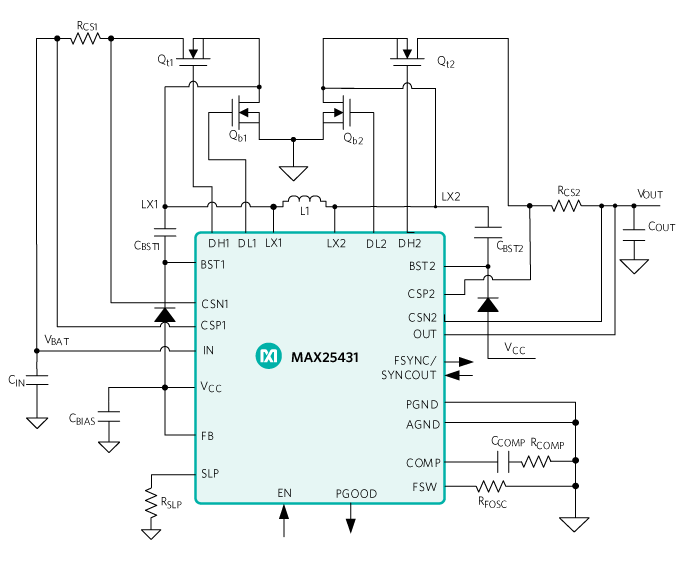
Figure 3. Buck-boost application diagram.
Higher Efficiency
In Figure 4, the IC delivers 3.5A with a peak efficiency of 98%. Compared to a competitor solution, the buck-boost controller exhibits an advantage of 2%, which is very critical in this application.
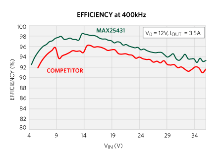
Figure 4. High-efficiency curve and comparison.
Low Temperature Rise
Figure 5 shows the PCB temperature distribution with VOUT = 20V, IPORTS = 3A, η = 96.29%, and 440kHz switching frequency, for a total output power PD = 2 x 60W (60W for each buck-boost).
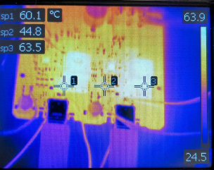
Figure 5. 120W PD solution thermal map.
The temperature rise is at most:
ΔT = 63.5 – 24.5 = 39°C
Superior efficiency and proper PCB design keep the temperature rise below 40°C even under this very extreme condition.
Small Size
The highly integrated controller yields a solution of only 2508mm2 area (Figure 6), 17% better than the closest competitor solution.
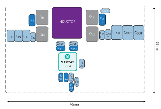
Figure 6. Small PCB size.
USB-PD Protection
Complementing the buck-boost controller is the MAX25410. The IC is an automotive USB-PD port protector solution for automotive radio, navigation, connectivity, and USB hub/multimedia module applications. The device provides a one-chip automotive USB-PD protection solution for the CC1, CC2, D+, and D- signals on a USB Type-C connector. The IC also provides a VCONN switch with advanced fault management that does not require a dedicated supply. The device protection features include ±15kV IEC 61000-4-2, ISO 10605 ESD, and short-to-VBUS (24V) on the protected HVCC1, HVCC2, HVD+, and HVD- pins. The device also has integrated BC1.2 charge-detection CDP, DCP, or pass-through (SDP) modes. The IC is available in a small 4mm x 4mm, 16-pin TQFN package.
Dual USB Type-C Power Delivery and Protection Module
The buck-boost solution and the protection IC are integrated into a USB-PD and protection module. Figure 7 shows a 120W high-efficiency, small-size power delivery module.

Figure 7. 120W high-efficiency, small-size power delivery module.
Conclusion
The USB-PD standard enables power delivery up to 60W with a standard cable, which raises the stakes in designing a dual USB module for automobiles since the allowed 40°C temperature rise is more challenging to achieve. On the signal side, the data lines must be adequately protected while supporting charge emulation and charge detection. The module must be easy to design and quick to reconfigure according to different customer platform requirements. After discussing the various challenges, we introduced a highly integrated chipset based on a buck-boost controller IC and a protection IC. We showed that with this chipset, the module temperature rise is contained within the allowed limit. Its small size makes the module cost-effective and easily adaptable to different form factors required by automobile manufacturers. The availability of ad-hoc solutions, complete with PCB, Allegro, and/or Gerber files helps in meeting crucial customer production deadlines.
Trademarks
USB Type-C is a registered trademark of the USB Implementers Forum, Inc. and Smart Power Selector is a trademark of Analog Devices Products, Inc.
{{modalTitle}}
{{modalDescription}}
{{dropdownTitle}}
- {{defaultSelectedText}} {{#each projectNames}}
- {{name}} {{/each}} {{#if newProjectText}}
-
 {{newProjectText}}
{{/if}}
{{newProjectText}}
{{/if}}
{{newProjectTitle}}
{{projectNameErrorText}}
最新视频 21


