Locating Shorts on Power Planes of Multi-Layer PCBs
Occasionally multi-layer PCBs arrive with power to ground shorts that are difficult to locate. Usually the response to questions about finding these shorts is to just “Hook it up to a 12V battery and find out where it smokes.” While this may work, it’s usually not desirable since the board will probably be destroyed during the test.
Another method of finding a short is by using a constant direct current source connected between the power and ground layers of the shorted power trace, probing the board with a microvolt meter and locating the short by finding the lowest voltage point on the board. This works with two layer boards where the power connection is generally accomplished by using thin traces which have milliohms of resistance, but is not effective where the power and ground are planes with resistances too small to allow a voltage reading. Also the power planes are usually buried in internal layers and are not accessible to test probes.
Once when asked to find a short on a prototype optical signal processing board costing approximately 80K$, I found a fairly simple, non-destructive method for locating the short.
Instead of using a direct current source, I used an alternating current source at a frequency in the audible range. Normally the AC field generated by this current is cancelled by the close proximity of the two planes conducting the current within the PCB. At the point where the short is located by a component on the board, the current is concentrated and disturbed in such a way as to result in a stronger AC field than is present at other points on the board. While bypass electrolytic caps present on the board will also conduct current, the ESR of these capacitors is generally orders of magnitude higher than that of the direct short.
If a small magnetic pickup loop is fabricated, fed to a high gain amplifier, and the output of this amplifier is connected to a pair of earphones, it is a fairly easy job to find shorts by simply moving the probe around the card until the strongest tone is heard. If the probe is small enough, the short can be isolated to a single pin on an IC.
While I used a high fidelity audio power amplifier and function generator to generate the signal, and a high gain phono preamp to amplify the signal from the pickup probe, it is possible to fabricate a couple of fairly simple circuits to perform the same function.
Current Generator and Loop Amplifier Circuit Description
To replace the audio power amplifier generating the audio signal, a multi-vibrator generating a square wave at approximately 800Hz is connected to a power amplifier stage with a current source output which is connected to the PCB. The circuit is powered by a 1.5V alkaline D cell to provide a 1A square wave of current.
Circuit Description, Current Generator
Q4 and Q5 form the multi-vibrator, Q3 and Q2 provide enough current gain to saturate Q1. R4 and the internal resistance of the battery limit the current provided to the PCB by Q1. The D cell has a 10 amp-hour capacity and the circuitry draws 0.5A. Since most tests take less than 5 minutes, the battery life should not be a concern.


Figure 1. 800Hz Square Wave Driver.
Circuit Description, Loop Receiver
The receiver must amplify the small signal from the single turn loop to a level sufficient to drive the headphones while not adding excessive noise. To effect this, a pair of low voltage noise LT1028 Operational Amplifiers are used to provide approximately 100 dB of gain.
U1 provides 57 dB of gain set by feedback resistors R3 and R1. C1 provides a high pass function at 300 Hz. This arrangement gives an overall gain of 1 at DC to prevent offset voltage from driving the output of the amplifier to the rail. C3 and R3 provide a low pass function at 1kHz. The purpose of this filtering is to limit excessive noise as well as filtering the detected square wave providing a more pleasing tone. R7-C5, R4-C4, and C6 provide further high pass and low pass filtering, and provide a DC gain of 1. R4-R2, set the gain of the second stage to 39dB to provide an overall gain of 96dB. Q1 provides current gain to drive the external headphones.

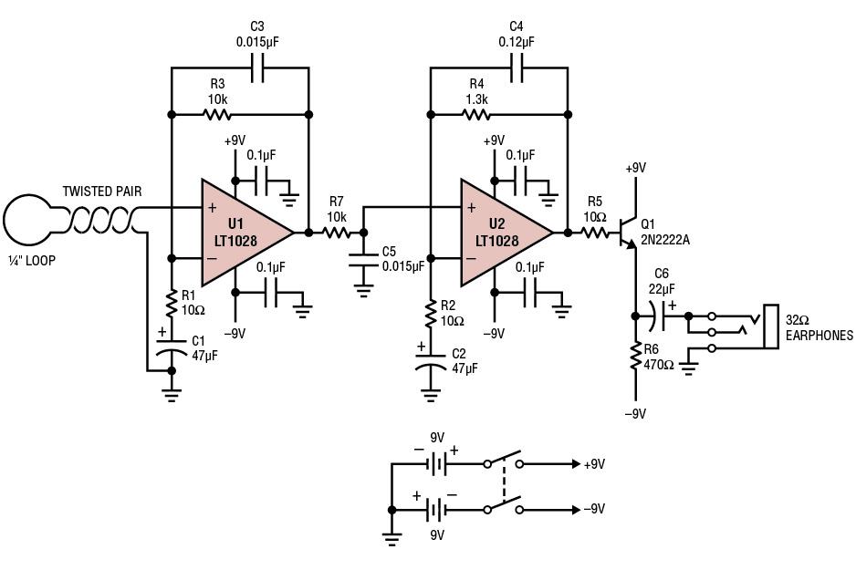
Figure 2. Magnetic Pick-Up Loop Amplifier.
Test Current Injection and Receiving Loop Details
The high current square wave is supplied to the power and ground to overcome external magnetic fields generated by power transformers and other extraneous sources of noise in close proximity to the receiving loop. The coupling between the field generated by the current generator and receiving circuitry must be minimized to achieve the sensitivity required to find a short. Leads from both the generator and the detection loop must be tightly twisted to minimize magnetic coupling between them. Braided shielding of the leads is not required since coupling is magnetic with minimal electric field. The signal generator leads must be connected as closely together as is possible to the edge of the board.
The receive loop I used was a quarter inch single loop fabricated from 30 AWG wire wrap wire. The wire wrap cable from the loop was tightly twisted for its entire length before being connected to the receiver. In use, with the generator connected, the receive loop is manipulated to different points on the board until an increase in the level of the tone received is detected. Moving closer to the short will increase the level of the tone. The small size of the loop allows accurate location of the short.
关于作者
关联至此文章
{{modalTitle}}
{{modalDescription}}
{{dropdownTitle}}
- {{defaultSelectedText}} {{#each projectNames}}
- {{name}} {{/each}} {{#if newProjectText}}
-
 {{newProjectText}}
{{/if}}
{{newProjectText}}
{{/if}}
{{newProjectTitle}}
{{projectNameErrorText}}
最新视频 21


