摘要
Linear regulators provide significant advantages over switching regulators in simplicity, cost, and output noise, but not efficiency. When applied to battery-operated portable equipment, battery life is more important than individual circuit efficiency, therefore, the choice between a low dropout (LDO) and a switching regulator is not so obvious. In addition, the particular battery characteristics, whether alkaline, NiCd, NiMH, or lithium (Li+), must be considered.
A similar version of this article appeared in the August, 1996 issue of Electronic Products.
Introduction
Advances in voltage-regulator design have helped to establish portable electronic products as the fastest growing segment of the electronics industry. The demands for low cost, long battery life, and small size in this market are changing and rearranging the design priorities for power supplies. The result is a general rewrite of specifications for the latest generation of power-supply ICs.
Surprisingly, both switch-mode and linear voltage regulators have participated in this transformation. Despite the predominant use of switch-mode regulators in portable products, the linear voltage regulator remains a viable contender. Advances in operating current, dropout voltage, noise, and packaging make the modern linear regulator very different from the LM309s and µA7805s used for most designs in the past.
Three very important questions must be asked when designing power supplies for portable products: Can a linear regulator work in my design? Will linear regulators (versus switching types) limit my battery life? Which regulator specs are critical? These questions are explored in the following discussion with an emphasis on portable and handheld applications. The issues discussed include a comparison of switch-mode and linear strengths, the parameters important to battery life, when linear regulators should not be used, how battery type can affect your design decisions, and how the characteristics of linear regulators can help or hinder a portable design.
Linear versus Switching Regulators
Before dealing with the subtleties of linear regulators for portable designs, it is worthwhile to make a comparison between the linear and switching types. In some cases, switching regulators can provide major benefits in a portable design. For example, if a high-performance switch-mode converter exhibits 90% efficiency (in transforming battery power to system power), then a linear design is unlikely to extend the battery life, unless the voltage differential between the battery and linear regulator is small.
Furthermore, the linear regulator can only step a voltage down to a lower level. If a system requires voltages not available from the battery, such as high voltage for a display or a negative voltage for analog circuitry, then the system usually requires switching regulators. Table 1 outlines the basic differences between linear and switch-mode regulators.
| Linear | Switching | |
| Function | Only steps down; input voltage must be greater than output | Steps up, steps down, or inverts |
| Efficiency | Low to medium, but actual battery life depends on load current and battery voltage over time; high if VIN - VOUT difference is small | High, except at very low load currents (µA), where switch-mode quiescent current (IQ) is usually higher |
| Waste Heat | High, if average load and/or input/output voltage difference are high | Low, as components usually run cool for power levels below 10W |
| Complexity | Low, which usually requires only the regulator and low-value bypass capacitors | Medium to high, which usually requires inductor, diode, and filter caps in addition to the IC; for high-power circuits, external FETs are needed |
| Size | Small to medium in portable designs, but may be larger if heatsinking is needed | Larger than linear at low power, but smaller at power levels for which linear requires a heat sink |
| Total Cost | Low | Medium to high, largely due to external components |
| Ripple/Noise | Low; no ripple, low noise, better noise rejection | Medium to high, due to ripple at switching rate |
There is generally a big advantage in using linear regulators instead of switchers when it comes to simplicity and cost, but not efficiency. However, the actual effect of measured efficiency on battery life can be deceptive. For many of the battery configurations to be discussed, linear-regulator efficiency is quite adequate when considered over the battery's full discharge cycle.
For very-low-power designs, even a large penalty in efficiency can be acceptable. In a handheld terminal, for example, a switching supply can be worth the cost if it increases battery life from 10 days to 15 days. For a small organizer, however, a similar expense just to increase battery life from 4 months to 6 months may not be justified.
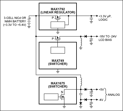
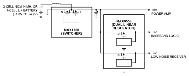
Combining linear and switch-mode regulators is a common technique for generating multiple supply voltages (Figure 1). A linear regulator (Figure 1a) converts battery voltage to a logic supply, and one or more switchers generate other voltages required for analog circuitry and liquid-crystal-display (LCD) bias. A different approach (Figure 1b) achieves noise and ripple rejection with a combination of linear and switch-mode regulators. Because power drawn by these regulators is not a major portion of the total load in a portable system, their effect on battery life is minimal.
(a)
(b)
Figure 1. (a) This handheld terminal uses linear regulation for the logic supply, but needs switch-mode converters for the LCD bias and analog circuitry. (b) In another application, a switch-mode boost converter is followed by linear postregulators for the low-voltage logic and RF receiver.
Will a Linear Regulator Suffice?
Linear regulators are preferred in most designs. Compared with switching regulators, they provide lower cost, fewer external components, and less circuit complexity. However, linear regulators have drawbacks: reduced battery life, higher cell count, larger dropout voltage, and heat. Though not unique to portable equipment, these problems call for solutions different from those associated with AC-powered equipment.
Cell count is often an inflexible issue in determining regulator type (or vice versa). Linear regulators, for example, require a sufficient number of series-connected cells to produce inputs that exceed the regulator's output voltage at all times. For a -3.3V output, this means using 3 or more cells (of roughly 1V to 1.5V each) for alkaline, NiCd, or NiMH batteries. Li+ batteries require fewer cells because Li+ cells have a higher voltage: usually between 2.5V and 4.2V. For 5V outputs, at least 5 cells may be needed to ensure a sufficient regulator input, as the cell voltages decline during discharge. For 12V outputs, the cell count becomes so high that a switch-mode boost converter often makes more sense than a linear regulator.
Linear regulators are most appropriate when the cell count is justified, from the standpoint of both voltage headroom and total energy. It is less sensible to satisfy a linear regulator's input requirement by stacking 5 or 6 cells, if only 2 cells have enough power to support the load for an adequate time. In that case, the added cost of a switch-mode boost converter can be justified by the lower cell count, particularly if the cells are rechargeable.
If the terminal voltage of a battery falls below the desired minimum, a linear regulator cannot extract all of the energy available as the battery nears its end of discharge. A switching regulator, however, can boost the battery voltage as required. But rather than incur the expense of a switcher, the designer often selects a linear regulator with the lowest available dropout voltage. (Dropout is the minimum allowed difference between the input and output voltages, which occurs just as regulation is lost.) Dropout voltages vary considerably for linear regulators, even among those labeled as low-dropout types by the manufacturer (Table 2).
| Pass Element | npn, Not Low Dropout | pnp, Low Dropout | pFET, Low Dropout | pFET, Low Dropout | pFET, Low Dropout |
| Example Part | LM78L05 | LP2952C | MAX8863 | MAX1589A | MAX883 |
| Typical Dropout Voltage (at 100mA Load) | 1.8V | 380mV | 110mV | 35mV | 110mV |
| Typical Quiescent (Ground) Current at No Load | 3mA | 75µA | 68µA | 70µA | 11µA |
| Quiescent Current vs. Load Current | Little change | Increases with load to 14mA (max) | No change | No change | No change |
| Quiescent Current in Dropout | Little change | 110µA at no load, increases with load | No change | No change | No change |
| Shutdown Current | Shutdown frequently not available | 75µA | 0.05nA | 0.01µA | 0.01µA |
| PSRR at High Frequencies | Good, about -42dB at 100kHz | Poor, about -12dB at 100kHz | Good, about -38dB at 100kHz | Good, about -42dB at 100kHz | Poor, about -10dB at 100kHz |
| Package | 8-pin SO | 8-pin SO | 5-pin SOT23 | 6-pin TDFN-EP | 8-pin SO |
Life with Real Batteries
A good starting point in designing a portable power supply is to consider the results obtained with a real battery, rather than an idealized power supply at the regulator's input. The characteristics fundamental to most batteries are a nonzero output resistance and the voltage decline associated with cell discharge (Figure 2). This discharge profile sometimes works in favor of linear regulation, because the power lost is a function of the input-output voltage difference.
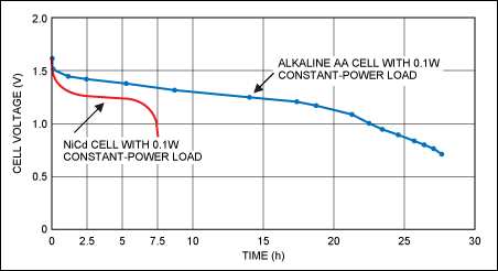
Figure 2. These curves illustrate typical alkaline- and NiCd-cell discharge profiles for a 100mW constant-power load. The NiCd cell's flatter discharge is due to its lower cell resistance.
Voltage is high and efficiency is poor for a freshly charged cell, but efficiency actually improves as the battery voltage drops (Figure 3). At dropout, when VIN nearly equals VOUT, the linear-regulator efficiency is almost 100%! This behavior is the opposite of that typical for switch-mode regulators. The important questions, though, are what efficiency level prevails for most of the battery's life, and what effect does this efficiency profile have on battery life? If the poorest efficiency lasts for a relatively short time, its impact on battery life may not be significant.
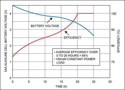
Figure 3. Efficiency increases as battery voltage declines for this 3-cell, linearly regulated system with a 100mW constant-power load. The average efficiency short of dropout is 85%. At dropout, approximately 5 hours of energy (20% of the total) are left in the battery, yielding a total cumulative efficiency of 68%.
Regarding the curves of Figure 3, as a downside, 20% of the energy (5 of 25 hours) remains in the battery when the regulator hits dropout. Thus the percentage of battery energy used, 85% × 80% = 68%, is still not bad for a low-cost design. The curves show that, if the system can be run in dropout down to 3.0V, raising the percentage of utilized battery energy to 85% × 90% = 76.5%, you can obtain another 2.5 hours of operation.
Better than Improving Efficiency
The least expensive method for improving efficiency in a portable design is reducing the load current, which increases the likelihood that a low-cost linear regulator can do the job. Though obvious, these benefits have no effect on the actual efficiency, which (by definition) is "power out divided by power in." Still, a reduction in load current can do more for battery life than a cutting-edge regulator design.
Consider the cost in finding a 10% improvement in power-supply efficiency, and then think about ways to reduce the load by the same 10% or more—with lower power ICs, by increasing pullup resistances, or with stingier power management by reducing the operating voltage. Often, money is better spent at the load than in the regulator. Reducing the output voltage in a linearly regulated system illustrates this point. In most cases, the battery life goes up because the ICs draw less current, but efficiency actually goes down ([(VOUT × IOUT)/(VIN × IIN)] decreases).
Why Care About Quiescent Current?
Another regulator specification critical in battery designs is quiescent current, also called "operating current" or "ground current." This current never makes it to the load; it flows from the battery to power the regulator itself. The importance of this spec is proportional to the magnitude of quiescent current with respect to load current. If load current is 350mA and quiescent current is 1mA, the quiescent contribution to inefficiency is only -0.28%. However for 1mA loads, the percentage loss is much worse: -50%.
Load currents often vary widely, so the net effect of quiescent current on battery life depends on a combination of these two cases. The question is, which load occurs for the greatest amount of time? If load currents are small for most of the time, then you must ensure a low quiescent current to achieve high efficiency. This caveat is especially critical in designs that never actually turn off. An instrument can have an on/off button, though "off" may only represent a sleep mode or standby state in which system power is active, but the load is in microamps. Table 3 shows how quiescent currents affect efficiency for three devices: a common low-power regulator often used in AC line-powered designs (the LM78L05), and two regulators optimized for low operating current (the MAX8863 and MAX882).
| Load Current (mA) |
Efficiency (%) (4.05V nom 3-Cell Input and 3.3V Output) |
||
| IQ = 3mA (LM78L05) |
IQ = 68µA (MAX8863) |
IQ = 11µA (MAX882) |
|
| 0.01 | 0.27 | 10 | 39 |
| 0.1 | 2.6 | 46 | 73 |
| 1 | 20 | 76 | 81 |
| 10 | 61 | 81 | 81 |
| 100 | 79 | 81 | 81 |
The behavior of quiescent current during dropout is a subtle but important difference between low-dropout (LDO) regulators based on pnp and pFET transistors (see columns 3 and 4 of Table 2). pFET gates draw virtually no current, so pFET regulators exhibit no quiescent rise during dropout. In the pnp design, however, quiescent current rises as the regulator struggles to maintain its output voltage by sinking base current to ground. For applications in which dropout is a normal occurrence rather than a "fault" condition (as in regulating 3 alkaline cells to 3.3V), this extra quiescent current can be significant.
If the system ICs allow a tolerance of ±10% in the supply voltage, it can be useful to keep operating as the output falls to 3.0V, draining the batteries to nearly 1V each. Devices based on pnp transistors tend to accelerate battery drain during this time by drawing more quiescent current. However, the quiescent current remains constant for FET-based regulators.
Heat
A major stumbling block for linear regulators in portable systems is the difficulty of dissipating heat from small enclosures. Thermal issues are important for any linearly regulated supply, but in portables (especially handheld devices), the problem becomes acute. Though ICs can handle only a limited amount of heat, the new surface-mount packages are helping. The 5-pin SOT23 package is rated for over 500mW, and some exposed-pad packages are rated for almost 2W (Table 4).
| Package | Standard 8-pin SO | 5-pin SOT23 | 8-pin µMAX®-EP | 6-pin TDFN-EP |
| Power Dissipation at +70°C (Ambient) | 444mW | 571mW | 1.3W | 1.95W |
| Thermal Resistance | 180°C/W | 140°C/W | 62°C/W | 41°C/W |
| Board Area (IC Only) | 31mm² | 9mm² | 15mm² | 9mm² |
| Height | 1.75mm | 1.45mm | 1.1mm | 0.8mm |
| Representative Part | LP2950 | MAX8863 | MAX1792 | MAX1589A |
New packages are introduced constantly, so it is good to monitor manufacturers' offerings. Figure 4 defines the usable average current as a function of input voltage for one 0.5A surface-mount device. Again, the load-current profile over time can act as a guide in dissipating the heat. If the load-current peaks are short enough to be integrated thermally, a lower power package can suffice.
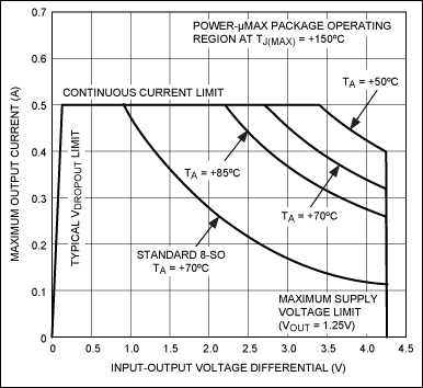
Figure 4. The MAX1792 comes in a high-power, 8-pin µMAX package with power dissipation exceeding that of a standard 8-pin SO. The safe operating area shows an inverse relationship between the maximum allowable output current and the magnitude of the input-output voltage differential.
Load Management
To reduce battery drain, many portable systems turn on their various internal circuit blocks only as needed. This switching is often implemented with logic-driven pFET switches following the regulated supply. To avoid losing regulation while delivering peak load currents, the FETs' on-resistance must be sufficiently low to ensure that the load-side voltage remains above the minimum level specified.
This switch-resistance problem is further complicated in low-voltage systems of 3.3V and below, because the low gate drive may not sufficiently minimize the FET's on-resistance. The cost of low-gate-threshold FETs is declining. However, in many cases, the use of multiple linear regulators offers a better approach. Many new linear regulators have a logic-level shutdown capability that turns off the regulator output completely, enabling the device to serve both as a regulator and a switch.
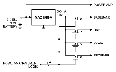
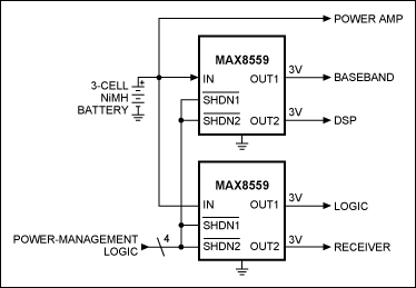
Figure 5 depicts a portable wireless product implemented with single (Figure 5a) and multiple (Figure 5b) regulators. The Figure 5b design is a bit more convenient if separate shutdown controls are provided for each output as shown, but it also works well with single-output devices. This design offers several advantages:
- It avoids two pass elements between the battery and the load (as is the case when the regulator is followed by FETs).
- It provides regulation on the output side of the regulator/switch.
- The regulators can be placed closer to their loads for better dynamic performance.
- The power dissipation is spread among two or more devices.
(a)
(b)
Figure 5. Two approaches to distributed power and load management in a portable wireless product are shown here. (a) A single regulator followed by pFET load switches requires low switch resistance. This ensures a regulated output while delivering peak load currents. (b) Two dual-regulator ICs perform the same function, but with two advantages: they provide four independently regulated outputs, and they distribute the power dissipation over multiple devices.
关联至此文章
产品
数字调节LCD偏置电源
1节至3节电池、大功率、低噪声、升压型DC-DC转换器
0.8A、低噪声、1MHz、升压型DC-DC转换器
500mA、低压差线性稳压器,µMAX封装
5V/3.3V或可调、低压差、低IQ、200mA线性稳压器,具有待机模式
5V/3.3V或可调、低压差、低IQ、500mA线性稳压器
双路、低压差、100mA线性稳压器
5V/3.3V或可调、低压差、低IQ、200mA线性稳压器,具有待机模式
双路、300mA、低噪声线性稳压器,带有独立的关断控制,UCSP或TDFN封装
5V/3.3V或可调、低压差、低IQ、500mA线性稳压器
低输入电压、500mA LDO稳压器,带有/RESET输出,SOT或TDFN封装
低压差、120mA线性稳压器
高效率、低电源电流、紧凑的、升压型DC-DC转换器
{{modalTitle}}
{{modalDescription}}
{{dropdownTitle}}
- {{defaultSelectedText}} {{#each projectNames}}
- {{name}} {{/each}} {{#if newProjectText}}
-
 {{newProjectText}}
{{/if}}
{{newProjectText}}
{{/if}}
{{newProjectTitle}}
{{projectNameErrorText}}
最新视频 21


