Easy-to-Use Spread Spectrum Clock Generator Reduces EMI and More
Introduction
The widespread proliferation of new portable electronic devices has created a problem for manufacturers and consumers alike: the potential for electromagnetic interference (EMI) between devices. EMI at minimum is a nuisance, as in the case of noise added to a television picture or a radio receiver. At worst, it can impair the operation of electronic devices in critical applications. EMI sources can be elusive, and thus hard to eradicate once a device is in the late stages of development. It behooves a device designer to proactively minimize the number of potential sources of EMI, possibly saving significant troubleshooting time down the road.
The amount of EMI generated, and whether it will produce significant interference, is not intuitively quantifiable. One way to quantify potential EMI problems is to test the conformance of the end product to various limits through procedures established by agencies such as CISPR (Comite International Special des Perturbations Radioelectriques).
If, at this point, excessive EMI is found, there is no need to panic. There are many techniques to significantly reduce radiated and conducted EMI in the end design, but few are as simple as using Spread Spectrum Frequency Modulation (SSFM) in the clocking of switching regulators.
Switching-regulators are increasingly prolific as power supply DC/DC converters in portable devices. Switching regulators owe their popularity in portable devices to their efficiency, which lengthens battery run time, but the rapid switching of current makes them a prime potential EMI source. If the frequency of the switcher is modulated via SSFM, however, the energy of the EMI is spread amongst many frequencies, instead of concentrated at one frequency. All that is needed is a clock that generates an SSFM signal to which the switcher can synchronize. The LTC6902 resistor programmable clock generator fills this need by randomly modulating its clock frequency.
Spread Spectrum Clocking
The idea behind using a spread spectrum technique to reduce EMI is to keep the clock moving. A steady clock is an easy target for neighboring devices and conformity test equipment to lock onto, allowing them time to accumulate emanating signal energy at the fixed clock frequency or its harmonics.
Figure 1 shows a comparison of spectra. This is a spectrum analyzer view of a square wave clock output from an LTC6902. Without SSFM, most of the signal energy in the output appears at the programmed 500kHz. With SSFM enabled, the output’s clock frequency shifts in a random fashion between 400kHz and 500kHz (a frequency change of 100kHz or 20% spreading). When applied to a switcher, the EMI energy at any particular high frequency has an amplitude one-tenth that of a single fixed clock frequency. These lower amplitude frequency components reduce the amount of potential interference.

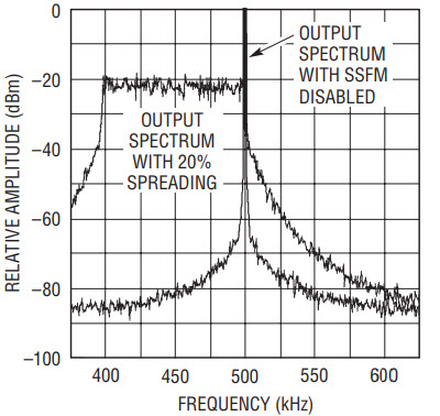
Figure 1. Clock output frequency spectrum with and without Spread Spectrum Frequency Modulation (SSFM)
How it Works
Figure 2 is a block diagram of the LTC6902. A single external resistor, RSET, establishes a current into the SET pin. This current fixes the frequency of a master oscillator block to any value within the range of 100kHz to 20MHz. The accuracy of this oscillator frequency is typically ±0.5% over the range from 500kHz to 10MHz. The master clock then passes through a programmable divider and multiphase circuit to provide from two to four clock output signals. By pin strapping the DIV (Divider) input to one of three voltage conditions (ground, open or V+) the master oscillator frequency is divided down by a factor of 1, 10 or 100. Use of this divider produces a wide output clock frequency range from 1kHz to 20MHz. Similar pin strapping of the PH (Phase) input controls the phase relationship of the output clock signals. The four clock output pins can be configured for two, three or four phase operation. Even without spread spectrum modulation, this level of versatility in clock generation is convenient for highly efficient multiphase switching regulator designs.

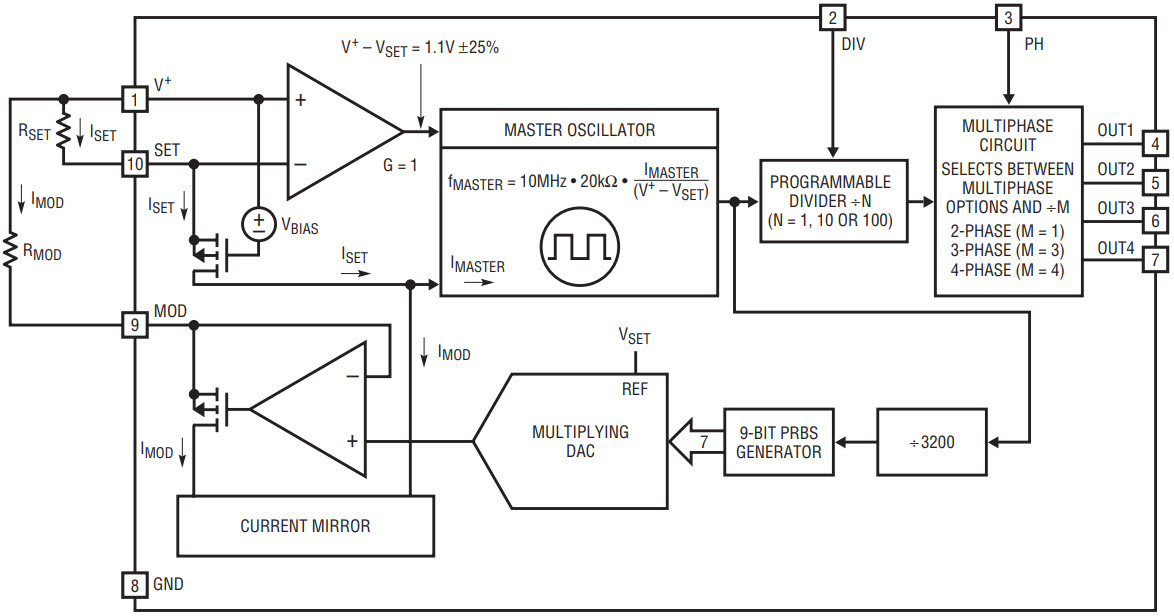
Figure 2. Functional block diagram of the LTC6902
The master oscillator also drives a pseudo-random binary sequence generator block. This block generates the random movement of the clock output frequency when spread spectrum is required. Seven bits of a 9-bit word drive a D-to-A converter which controls the magnitude of a current that is subtracted from the master oscillator set current. This modulation of the master oscillator current, and therefore the output frequency, results in 128 random values. A second resistor, RMOD, sets the range of this frequency spreading. The lowest output frequency occurs when the DAC receives a zero-scale input code and the maximum IMOD current is subtracted from ISET.
The design equations to control the operation of the LTC6902 are very simple. The resistor value chosen for RSET controls several characteristics. The master oscillator frequency;
The value for RSET should be in the range of 10k to 2MΩ to obtain the most accurate master oscillator frequency.
The master oscillator frequency in turn fixes the Spread Spectrum Modulation frequency and frequency change time interval;
and
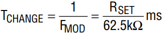
Since minimizing EMI is the reason behind spread spectrum clocking, the master oscillator does not respond instantaneously to each change in frequency. The internal control loop for establishing the operating frequency has a 25kHz bandwidth. This serves to soften the transitions and greatly reduce higher frequency spurs. Keeping the value for RSET between the recommended limits also ensures that the clock update rate does not exceed the built in control loop bandwidth limit.
RSET also controls the frequency change pattern repeat interval as follows:
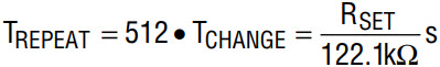
As mentioned previously the modulation pattern is a pseudo-random binary sequence and repeats itself every 512 clock frequency changes. Figure 3 shows the voltage measured at the MOD pin. This is the output voltage of the D to A converter as it modulates the current supplied to the master oscillator.

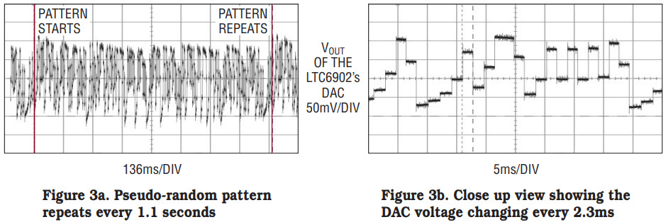
Figure 3. The pseudo-random output of the LTC6902’s DAC is used to modulate the output frequency.
With the MOD ping rounded, spread spectrum operation is disabled and the LTC6902 serves as a multi-phase clock generator. The value of RSET and the selection of the master oscillator divide factor and the number of clock phases determine the output clock frequency. This is also the maximum output frequency and is determined as follows:
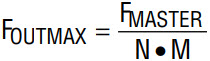
where N is the master oscillator divide factor of 1, 10 or 100 and M is set by the desired phasing of the output clock signals to be either 1, 3 or 4 for two, three or four phases respectively. Through combinations of the these three controls, a desired maximum output frequency can be derived from different master oscillator frequencies which results in different clock change intervals and pattern repeat times.
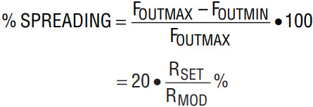
Resistor RMOD sets the range of clock frequencies generated by the pseudo-random DAC output signal. The output frequency always spreads down from FOUTMAX. The reason down spreading is preferred stems from the possible use of the output clocks to strobe logic devices. If device timing requirements such as data set-up and hold time are met at the maximum clock rate, then proper operation at lower frequencies is a given. The ratio of RSET to RMOD controls the range of frequencies generated. Expressed as a percent of FOUTMAX the output frequency spreading range is set by the following relationship:
A practical range of frequency spreading is from 0% to 80% of FOUTMAX. The amount of desired frequency spreading varies by application, but is easily adjusted via a single resistor value, making it easy to fine tune the EMI performance.
Clocking a Switching Regulator
The most common use of the LTC6902 is with switching voltage regulators. Regulators that have a SYNC or CLOCK input pin can be controlled by an external clock source. Multiple regulators in a system can all be driven from the same source in order to be synchronized to the same frequency. This makes it much easier to control radiated and conducted EMI through both filtering and frequency spreading.
By employing frequency spreading, overall system compliance to EMI standards can be met. While spreading actually creates new components of signal energy over a range of frequencies, the amplitudes of these are much lower than the spikes in a fixed frequency design. A typical design is shown in Figure 4. The LTC6902 clocks the SYNC pin of an LT3430, a 2A, step-down switching regulator, at 570kHz. This value was arbitrarily chosen at a frequency greater than the 250kHz internal clock of the regulator. The regulator provides a 5V output at 2A from an 8V to 42V input supply with greater than 80% efficiency.

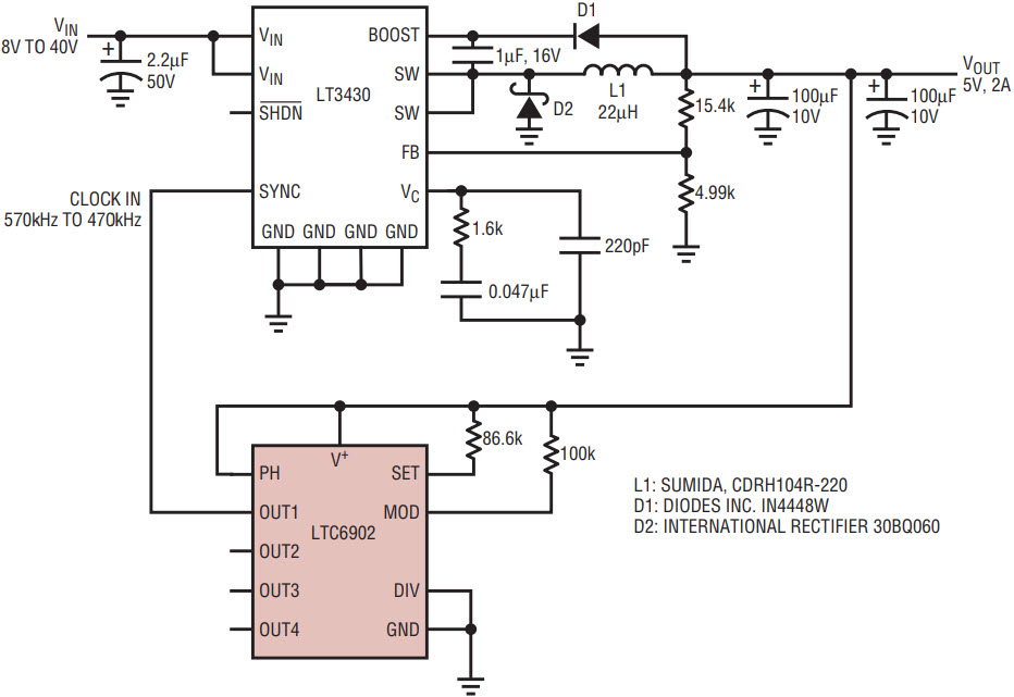
Figure 4. Spread spectrum modulation clocking of a switching regulator. Example circuit for a high-efficiency, 5V, 2A regulated output.
Figure 5 shows the fundamental benefit of spread spectrum clocking. This is the spectrum of the conducted input current to the switcher at a full 2A load both with and without frequency spreading. The measurement was made to a CISPR compliance standard for the frequency band of 150kHz to 30MHz using a quasi-peak measurement technique. Without spreading, the energy at the fundamental clock frequency clearly fails the compliance limit, as shown in Figure 5a. The harmonics of the clock frequency also approach the test limit. In contrast, Figure 5b shows that by using the LTC6902 to spread the frequency, the amplitude of the fundamental component is reduced by 30dB to a value below the compliance recommendation. In this case, spreading was set to be 17% resulting in a clock frequency range from 470kHz to 570kHz. The system now passes EMI compliance.

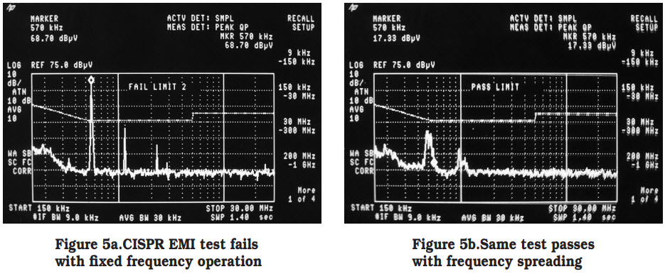
Figure 5. EMI compliance success! CISPR test of the conducted input current of the circuit in Figure 4, for the 150kHz to 30MHz frequency band.
The rate of change of frequency is an important consideration when using SSFM with a switching regulator. Although changing the clock frequency as quickly as possible minimizes interference, there is a limit to how fast you can change the frequency of a switching regulator. It is important that the bandwidth of the regulator feedback loop be wide enough to allow it to adjust quickly to a new clock frequency. As shown in Figure 6, if the clock changes too fast for the switcher to respond, the output of the regulator can appear unstable, which can result in increased ripple and loss of regulation as it tries to adjust to a new clock frequency. Operating with a slower master oscillator frequency and proper selection of the divide factor and output phase settings can slow the output frequency change rate of the LTC6902 to manageable levels.

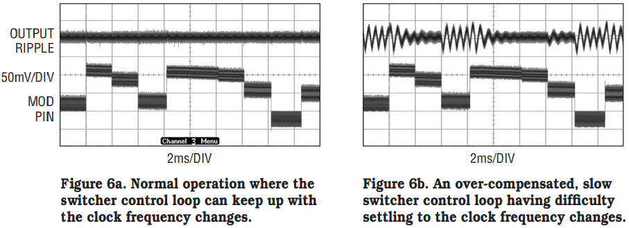
Figure 6. The rate of change of the clock frequency can be a problem if it is too fast for the loop response of a switching regulator.
Spread Sampling
In addition to EMI improvement, spread spectrum techniques can also minimize the effects of aliasing in high-accuracy data acquisition systems. Figure 7 shows the LTC6902 providing the external conversion clock input to an LTC2410, 24-bit ΔΣ ADC. The LTC2410 has a built in very sharp 4th order Sinc filter to notch out 50/60Hz interference input signals by more than 100dB resulting in extremely accurate DC precision. The 60Hz notch occurs when the external clock applied is set to 153.6kHz, which also sets the delta sigma modulator sampling frequency to 15.36kHz. Being a sampling system, however, means that aliasing can occur. Input signal content such as noise in a narrow band, approximately 12Hz, around 15.36kHz will fold back and create a near DC frequency component that is indistinguishable from valid input signals. This can cause conversion errors.

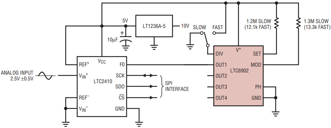
Figure 7. Reduce aliasing in ADCs. Here, the LTC6902 drives an LTC2410 Delta Sigma converter to spread the sampling rate.
By modulating the clock frequency with the LTC6902, signal aliasing becomes a moving target. Input signal energy near a particular sample rate of the converter is folded back only for the short time that sample rate occurs before moving to a new value. Each conversion of the LTC2410 takes approximately 120ms. If the clock is modulated at a 5kHz rate it only sits at any given frequency for 200µs, a small percentage of the conversion time. Any aliasing tone will only have this short time to impair the complete conversion result.
Figure 8 illustrates the effect of sample rate modulation. For these measurements a 1VP–P input signal was applied to the converter and swept in frequency through the sample rate in order to force aliasing and observe the results. With no spreading and the sample rate fixed at 15.36kHz, the aliasing conversion error is large but confined to the range of frequencies very near the sampling rate. This also shows the sharp attenuation characteristics of the sinc filter.

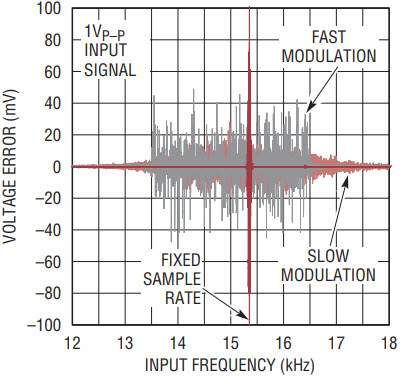
Figure 8. Error voltage measurement caused by forced aliasing. Three test runs show the effects with a fixed sampling frequency, a slow modulation rate and a fast modulation rate.
With slow modulation of the sample rate over a range of 12.5kHz to 17.5kHz the aliasing is much lower in amplitude but occurs at more frequencies. For this test, the master oscillator of the LTC6902 was set to 165kHz. This makes the clock change every 20ms and the entire pattern repeat every 10 seconds. More spurs appear because the sample rate, as it randomly moves about, occasionally matches the input signal frequency, thus forcing frequency fold back. Nevertheless, the amplitudes of the spurs are significantly lower than the amplitude of the spike at the at the fixed frequency sampling rate. This is because the foldback condition is ephemeral, lasting much less than the conversion time of the LTC2410.
A third test has the clock or sample rate varying over the same frequency range but changing at a one hundred times faster rate. The LTC6902 is programmed for a master oscillator frequency of 16.5MHz for a frequency change rate of 200µs and a pattern repeat interval of 100ms. The divide by 100 setting is applied to set the maximum converter sample rate at 16.5kHz. This arrangement lowers the aliasing error even more, but spurs appear over the entire sampling frequency range. This is because the repeat interval is shorter than the conversion time. The sample frequency is guaranteed to match the input frequency at least once during every conversion but for a very short interval.
Spread spectrum sampling of high resolution ADCs has merit in reducing the magnitude of measurement errors caused by aliasing. The trade-off, however, is the potential of introducing errors by extending the range of frequencies that can fold back.
Conclusion
The LTC6902 is an easy-to-use resistor programmable oscillator, which, with selectable output phases, can serve as a simple non-overlapping clock generator. It’s powerful additional feature, however, is that it can randomly modulate the output frequency to implement spread spectrum clocking. Spread spectrum clocking is a simple solution to reducing power supply EMI to standards compliance, where otherwise the application would require significant and costly redesign.
关于作者
最新视频 21


