摘要
This application note discusses the timing requirements for the commonly used serial asynchronous communications protocol implemented in UARTs. The article shows how to determine the tolerance for the UART clock source at both ends of an asynchronous link.
Background
The RS-232 specification dates back to 1962, when it was first released by the Electronic Industries Alliance (EIA). The specification has changed over time, incorporating higher data rates and closing the compatibility gaps between the Telecommunications Industry Association (TIA), International Telecommunication Union (ITU), and International Standards Organization (ISO) requirements. The current version of the RS-232 specification is EIA/TIA-232-F, issued in October 1997.
RS-232 benefited from the availability of MSI ICs from the late 1970s, which had the complexity to handle the specification at a reasonable cost. These ICs are universal asynchronous receive transmitters (UARTs). Many large-scale integration (LSI) ICs (including microcontrollers) now include the functionality.
As is often the case, the availability of UARTs drove the industry to use the RS-232 serial protocol in non-RS-232 ways. Common examples are RS-485 transmissions, optoisolated transmissions, and transmissions using a single-ended physical layer (that is, 0 to 3.3V instead of ±5V or ±10V). This article covers the general timing aspects of the serial interface, not application nuances of handshaking or the physical layer. Therefore, the application note is applicable to all generalized UART applications.
UART Timing
A typical UART frame is shown in Figure 1. It comprises a START bit, 8 data bits, and a STOP bit. Other variants are also possible in RS-232 applications. For example, the data packet could be 5, 6, or 7 bits long, there could be 2 STOP bits, or a parity bit could be inserted between the data packet and the STOP bit for rudimentary error detection. Figure 1 shows the signaling as seen at a UART's transmit data (TXD) or receive data (RXD) pins. RS-232 bus drivers invert as well as level shift, so a logic 1 is a negative voltage on the bus and a logic 0 is a positive voltage.
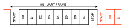
Figure 1. A typical UART data frame.
When two UARTs communicate, it is a given that both transmitter and receiver know the signaling speed. The receiver does not know when a packet will be sent (no receiver clock); hence, the protocol is termed "asynchronous." The receiver circuitry is correspondingly more complex than that of the transmitter. The transmitter simply has to output a frame of data at a defined bit rate. Contrastingly, the receiver has to recognize the start of the frame to synchronize itself, and therefore determine the best data-sampling point for the bit stream.
Figure 2 shows a common method used by a UART receiver to synchronize itself to a received frame. The receive UART uses a clock that is 16 times the data rate. A new frame is recognized by the falling edge at the beginning of the active-low START bit. This occurs when the signal changes from the active-high STOP bit or bus idle condition. The receive UART resets its counters on this falling edge, expects the mid-START bit to occur after 8 clock cycles, and anticipates the midpoint of each subsequent bit to appear every 16 clock cycles thereafter. The START bit is typically sampled at the middle of bit time to check that the level is still low and ensure that the detected falling edge was a START bit, not a noise spike. Another improvement is to sample the START bit three times (clock counts 7, 8, and 9, out of 16) instead of sampling it only at the midbit position (clock count 8 out of 16).
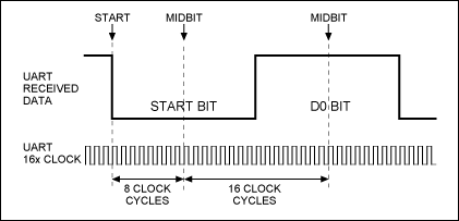
Figure 2. UART receive frame synchronization and data sampling points.
Timing Accuracy
How accurate must the receive UART clock be to receive data correctly? Since the absolute clock rate is unimportant for the purposes of accurate reception, a better question would be to ask how different the transmit and receive UART clocks can be. The first point to understand is that because the UART receiver synchronizes itself to the start of each and every frame, we only care about accurate data sampling during one frame. There is no buildup of error beyond a frame's STOP bit, which simplifies analysis because we only have to consider one frame for the worst-case scenario.
When do we get a timing error due to transmit-receive clock mismatch? Our goal is to sample each bit at the midpoint (Figure 2). If we sample one-half a bit-period too early or too late, we will be sampling at the bit transition and have problems (Figure 3).
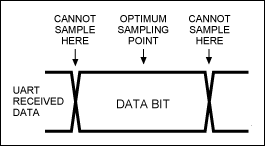
Figure 3. UART receive sampling range.
In reality, we cannot sample close to the bit-transition point reliably. The primary reason for this is the finite (and typically slow) transmission rise and fall times. These times become even slower if overly capacitive cabling is used. A long bus incurs high attenuation, which reduces noise margin and makes it more important to sample when the bit level has settled.
It is difficult to quantitatively assess a worst-case acceptable sampling range across a bit's period. EIA/TIA-232-F does specify a 4% of bit-period maximum slew time for a transmission, but this is difficult to achieve for long runs at 192kbps. But for the purpose of this application note, let us define two data path scenarios. Consider a "nasty" scenario, which can only be sampled reliably within the middle 50% of the bit time (Figure 4). This could equate to a long capacitive RS-232 run. The "normal" scenario can be sampled within the middle 75% of the bit time (Figure 5). This equates to a relatively benign bus (such as a meter-length bus with buffered CMOS logic levels or an RS-485 differential pair) within an equipment chassis.
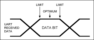
Figure 4. UART "nasty link" is sampled reliably within 50% of bit time.
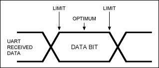
Figure 5. UART "normal link" is sampled reliably within 75% of bit time.
For Figures 4 and 5, we can determine that the error budget is ±25% and ±37.5% from the optimal bit-center sampling point for the nasty and normal scenarios, respectively. This error is equivalent to ±4 or ±6 periods of the 16x UART receive clock. Another error to include in this budget is the synchronization error when the falling edge of the START bit is detected. The UART will most likely start on the next rising edge of its 16x clock after detecting the START-bit. Since the 16x clock and the received data stream are asynchronous, the falling edge of the START bit could occur just after a 16x clock rising edge. The falling edge could, alternatively, occur just before the clock rising edge, but not with enough setup time to use it. This means that the UART has a ±1 bit error built in at the synchronization point. So our error budget reduces from ±4 or ±6 clock periods to ±3 or ±5 periods.
We will presume that short-term clock errors (essentially jitter) are very small, and therefore we are only considering midterm and long-term errors. These errors point to a mismatch in the transmit UART and receive UART timing that is consistent during a frame. Since the timing is synchronized at the falling edge of the START bit, the worst-case timing error will be at the last data sampling point, which is the STOP bit1. The optimum sampling point for the STOP bit is its bit center, which is calculated as:
(16 internal clock cycles per bit) × (1 start bit + 8 data bits + ½ a stop bit) = (16) × (9.5) = 152 UART receive clocks after the original falling edge of the START bit.
Now we can calculate our allowable error as a percentage. For the normal scenario, the clock mismatch error can be ±5/152 = ±3.3%. For the "nasty" scenario it can be ±3/152 = ±2%. As hinted earlier, although the problem will materialize at the receive end of the link, clock mismatch is actually a tolerance issue shared between the transmit and receive UARTs. So presuming that both UARTs are attempting to communicate at exactly the same bit rate (baud), the allowable error can be shared, in any proportion, between the two UARTs.Making use of the allowable error budget is helpful in systems where both ends of the link are being designed at the same time. This is partly because the tolerance of both ends will be known, and partly because trade-offs and cost savings can be made. In general, a standard low-cost, ceramic resonator with ±0.5% accuracy and a further ±0.5% drift over temperature and life can be used for the clock source at both ends of the link. This meets the 2% "nasty" scenario discussed earlier. If the system uses a master controller (typically a microcontroller or a PC) with a standard 100ppm crystal oscillator for the UART clock source, the link error can be cut approximately in half. Be careful with microcontrollers that synthesize baud frequencies for their internal UARTs. Depending on the choice of microcontroller clock, the baud rates may not be exact. If the error can be determined, it can be easily included in the link error budget.
It may appear odd that the STOP bit is sampled, but it is. If the STOP bit is detected as a low level instead of the expected high level, UARTs typically report a frame error.
关联至此文章
产品
低电容、2/3/4/6通道、±15kV ESD保护阵列,用于高速数据接口
低电容、2/3/4/6通道、±15kV ESD保护阵列,用于高速数据接口
低电容、2/3/4/6通道、±15kV ESD保护阵列,用于高速数据接口
四通道串行UART,具有128字FIFO
SPI/I²C UART,具有128字FIFO
SPI/MICROWIRE兼容的UART及±15kV ESD保护、RS-232收发器,内置电容
SPI/MICROWIRE兼容UART
SPI/MICROWIRE兼容的UART及±15kV ESD保护、RS-232收发器,内置电容
SPI/MICROWIRE兼容的UART,集成真正失效保护的RS-485/RS-422收发器
带0.1µF外部电容的+5V、RS-232收发器
+5V供电、多通道RS-232驱动器/接收器
+5V供电、多通道RS-232驱动器/接收器
+5V供电、多通道RS-232驱动器/接收器
带0.1µF外部电容的+5V、RS-232收发器
+5V、RS-232收发器,0.1µF外部电容
+3.0V至+5.5V、10nA、250kbps RS-232收发器,带有±15kV ESD保护、输入/输出和逻辑引脚
±15kV ESD保护、+2.5V至+5.5V、RS-232收发器,UCSP和WLP封装
±15kV ESD保护、+5V RS-232收发器
±15kV ESD保护、1µA、1Mbps、3.0V至5.5V、RS-232收发器,提供AutoShutdown Plus
3.0V至5.5V、低功耗、1Mbps、真RS-232收发器
+5V供电、多通道RS-232驱动器/接收器
1µA电源电流、1Mbps、3.0V至5.5V、RS-232收发器,提供AutoShutdown Plus
+5V、RS-232收发器,0.1µF外部电容
+5V供电、多通道RS-232驱动器/接收器
+5V供电、多通道RS-232驱动器/接收器
+5V、1µA、单路RS-232收发器,带有AutoShutdown
低功耗、AppleTalk™接口收发器
±15kV ESD保护、+5V RS-232收发器
+3.0V至+5.5V、1µA、高达250kbps、真RS-232收发器,提供AutoShutdown Plus
±15kV ESD保护、1µA、1Mbps、3.0V至5.5V、RS-232收发器,提供AutoShutdown Plus
+2.5V至+5.5V、RS-232收发器,UCSP封装
±15kV ESD保护、1µA、3.0V至5.5V、250kbps RS-232收发器,带有AutoShutdown
±15kV ESD保护、1Mbps、1µA RS-232发送器,SOT23-6封装
1µA电源电流、1Mbps、3.0V至5.5V、RS-232收发器,提供AutoShutdown Plus
±15kV ESD保护、+5V、1µA、单路RS-232收发器,带有AutoShutdown
+5V供电、多通道RS-232驱动器/接收器
+5V、RS-232收发器,0.1µF外部电容
±15kV ESD保护、12V、双路RS-232串口,带有低功耗待机模式,适用于主板/台式机
+5V供电、多通道RS-232驱动器/接收器
+5V供电、多通道RS-232驱动器/接收器
+5V供电、多通道RS-232驱动器/接收器
±15kV ESD保护、1Mbps、1µA RS-232发送器,SOT23-6封装
1µA电源电流、1Mbps、3.0V至5.5V、RS-232收发器,提供AutoShutdown Plus
±15kV ESD保护、1µA、3.0V至5.5V、250kbps RS-232收发器,带有AutoShutdown
1µA电源电流、+3V至+5.5V、真RS-232收发器,带有AutoShutdown
±15kV ESD保护、1µA、250kbps、3.3V/5V、双路RS-232收发器,内置电容
±15kV ESD保护、电流低至10nA、3.0V至5.5V供电、速率高达1Mbps的真RS-232收发器
1.8V至4.25V供电、双路、真RS-232收发器
+5V、RS-232收发器,0.1µF外部电容
+3.0V至+5.5V、10nA、250kbps RS-232收发器,带有±15kV ESD保护、输入/输出和逻辑引脚
+5V供电、多通道RS-232驱动器/接收器
+5V供电、多通道RS-232驱动器/接收器
±15kV ESD保护、+5V RS-232收发器
±15kV ESD保护、电流低至10nA、3.0V至5.5V供电、速率高达1Mbps的真RS-232收发器
±15kV ESD保护、460kbps、RS-232发送器,SOT23-6封装
±15kV ESD保护、+5V RS-232收发器
3.0V至5.5V、低功耗、1Mbps、真RS-232收发器
±15kV ESD保护、+5V RS-232收发器
+5V供电、多通道RS-232驱动器/接收器
3.0V至5.5V、低功耗、1Mbps、真RS-232收发器
+5V、RS-232收发器,0.1µF外部电容
±15kV ESD保护、1µA、1Mbps、3.0V至5.5V、RS-232收发器,提供AutoShutdown Plus
±15kV ESD保护、1µA、1Mbps、3.0V至5.5V、RS-232收发器,提供AutoShutdown Plus
+5V供电、多通道RS-232驱动器/接收器
+3V供电、低功耗、真RS-232收发器
±15kV ESD保护、电流低至10nA、3.0V至5.5V供电、速率高达1Mbps的真RS-232收发器
±15kV ESD保护、+5V RS-232收发器
±15kV ESD保护、+2.5V至+5.5V、RS-232收发器,UCSP和WLP封装
1µA电源电流、1Mbps、3.0V至5.5V、RS-232收发器,提供AutoShutdown Plus
+5V供电、多通道RS-232驱动器/接收器
+2.5V至+5.5V、RS-232收发器,UCSP封装
+5V供电、多通道RS-232驱动器/接收器
1µA电源电流、+3V至+5.5V、真RS-232收发器,带有AutoShutdown
+5V供电、多通道RS-232驱动器/接收器
±15kV ESD保护、460kbps、RS-232发送器,SOT23-6封装
+5V、RS-232收发器,0.1µF外部电容
+5V供电、多通道RS-232驱动器/接收器
+5V、RS-232收发器,0.1µF外部电容
1Mbps、1µA RS-232发送器,SOT23-6封装
±15kV ESD保护、1µA、1Mbps、3.0V至5.5V、RS-232收发器,提供AutoShutdown Plus
1µA电源电流、1Mbps、3.0V至5.5V、RS-232收发器,提供AutoShutdown Plus
1µA、1.8V至4.25V、RS-232收发器,带有AutoShutdown™
+5V、RS-232收发器,0.1µF外部电容
±15kV ESD保护、电流低至10nA、3.0V至5.5V供电、速率高达1Mbps的真RS-232收发器
+5V供电、多通道RS-232驱动器/接收器
+5V供电、多通道RS-232驱动器/接收器
+5V供电、多通道RS-232驱动器/接收器
+5V供电、多通道RS-232驱动器/接收器
+5V供电、多通道RS-232驱动器/接收器
1Mbps、1µA RS-232发送器,SOT23-6封装
3.0V至5.5V、低功耗、1Mbps、真RS-232收发器
1µA电源电流、+3V至+5.5V、真RS-232收发器,带有AutoShutdown
+5V、RS-232收发器,0.1µF外部电容
+5V供电、多通道RS-232驱动器/接收器
±15kV ESD保护、1µA、1Mbps、3.0V至5.5V、RS-232收发器,提供AutoShutdown Plus
+5V供电、多通道RS-232驱动器/接收器
±15kV ESD保护、1µA、3.0V至5.5V、250kbps RS-232收发器,带有AutoShutdown
+5V供电、多通道RS-232驱动器/接收器
+5V、RS-232收发器,0.1µF外部电容
可编程DTE/DCE、+5V、RS-232收发器
±15kV ESD保护、+5V RS-232收发器
±15kV ESD保护、+5V RS-232收发器
±15kV ESD保护、1µA、250kbps、3.3V/5V、双路RS-232收发器,内置电容
±15kV ESD保护、电流低至10nA、3.0V至5.5V供电、速率高达1Mbps的真RS-232收发器
±15kV ESD保护、+5V RS-232收发器
±15kV ESD保护、+5V RS-232收发器
1µA电源电流、1Mbps、3.0V至5.5V、RS-232收发器,提供AutoShutdown Plus
+2.7V至+3.6V供电、1µA电源电流、3驱动器/5接收器、真RS-232收发器
低电容、2/3/4/6通道、±15kV ESD保护阵列,用于高速数据接口
最新视频 21


