摘要
Inductor-based switch-mode power supplies can take significant design effort and increase size, especially for generating negative supply currents for op amps or LCD bias. This application note describes how a switch-mode power-supply controller such as the MAX774 and a diode-capacitor network can generate modest negative supply currents without the use of inductors.
A switch-mode power-supply controller and diode-capacitor network can generate the modest negative supply currents required for op amps or for LCD bias, without the design effort and size penalty associated with inductors (Figure 1). The circuit of Figure 1 accepts inputs of 2V to 6V and produces a digitally adjustable output voltage. The diode-capacitor charge pump is driven by the switching action of DHI and DLOW, which normally drive an external MOSFET or pnp transistor in an inductor-based switch-mode power supply.
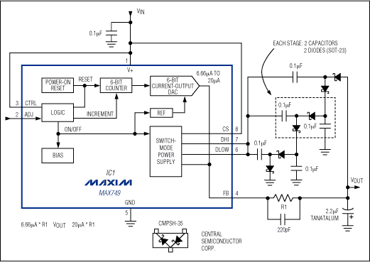
Figure 1. Driving a diode-capacitor network instead of an inductor, this DC-DC controller IC produces a regulated negative output with modest IOUT capability.
At power-up, the internal 6-bit current-output D/A converter produces a nominal VOUT of R1 x 13.33µA. Then, by holding CTRL high and toggling ADJ, you can adjust VOUT over a 3:1 range in 64 equal steps, according to the value of R1: R1 x 6.66µA ≤ VOUT ≤ R1 x 20µA. If digital adjustment is not required, ground the ADJ pin and connect CTRL to V+. Or construct a similar circuit with the MAX774 DC-DC controller, which accepts inputs up to 16.5V. For positive outputs greater than VIN, a step-up controller and modified charge-pump network (not shown) can do the job.
The maximum output current depends on VIN, VOUT, and the number of diode-capacitor stages, each of which consists of two diodes and two capacitors. Though only a few microamps are available at the maximum VOUT, which equals VIN - (0.6V x the number of stages), you can draw more current at the lower output voltages (Figure 2).
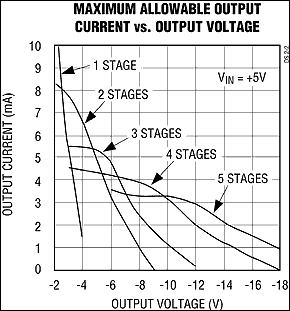
Figure 2. The available output current in Figure 1 depends on VIN (5V for this graph), VOUT, and the number of diode-capacitor stages.
The number of diode-capacitor stages determines the maximum IOUT for a given VIN and VOUT. Too few stages will not achieve the desired voltage, but too many degrades the efficiency: IIN equals (approximately) IOUT times the number of stages. For VIN less than 5V, the circuit delivers less output current than is indicated by the curves of Figure 2. For example, a 4-stage circuit produces an output current of 1mA at -2V out from 2VIN, at -7V from 3VIN, at -11V from 4VIN, and at -14.5V from 5VIN. Larger pump capacitors can provide higher IOUT.
The controller changes its behavior when VOUT is much lower than the voltage programmed by R1. Designed for inductor-based circuits, it compensates for impending dropout by increasing the switching transistor's "on" time at the expense of "off" time. This action normally ramps up the inductor current, but it has an opposite effect for the circuit shown. Because short off times (DHI high) don't allow the capacitors to discharge fully, the available output current actually decreases instead of increasing. Thus, when VOUT loses regulation due to overload, you must reduce the load current considerably before regulation can be regained. A reliable maximum output current is the level at which VOUT recovers from dropout, not the higher level at which it enters dropout.
For stable operation, bypass R1 with 220pF, keep the connections between R1 and IC1 very short, and place the input bypass capacitor directly across the input pins of IC1. Output ripple is typically less than 1% for the component values shown, but ripple can be higher if the circuit includes more stages than that required by the programmed output voltage. Ripple can be lowered by increasing the output capacitance.
最新视频 21


