轻松完成控制回路仿真
摘要
本文介绍了一种进行控制回路仿真的简便方法,使用LTspice®可以轻松生成波特图。
引言
在设计电源时,仔细检查控制回路至关重要。控制回路设置不当可能会导致电源转换器振荡或运行不稳定。这种振荡不仅会在输出端产生过高的电压纹波,还会降低电磁兼容性(EMC)性能。此外,倘若控制回路设置不合理,电压转换器对负载瞬变和电源电压变化的响应速度也会变慢。
检查控制回路的简单步骤
波特图为检查控制回路提供了一个有用的依据。借助诸如 LTspice (17.1版本或更高版本)等仿真工具,可以轻松、快速地 生成波特图。本文将探讨进行波特图仿真的三个步骤。
第一步,使用LTspice打开电源电路,例如一个开关稳压器电 路。图1显示了 ADP2370降压型开关稳压器的电路。在LTspice中,测试电路(也就是外部电路)可以从现成的电路中选择。当电路出现在显示屏上后,从“组件”选项卡中选择一个频率响应分析仪(FRA)。它将添加至上分压电阻(R1)的上方。图1显示了本例中所使用的FRA。
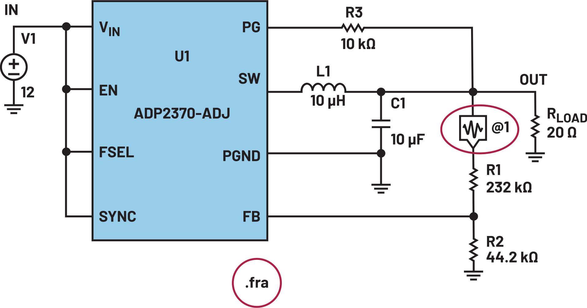
图1. 在开关稳压器电路中添加频率响应分析仪,以便进行波特图仿真。
接下来,选择一种用于生成波特图的仿真类型。在图1中,仿真类型显示为“.fra”。
在开始波特图仿真之前,必须输入所需的参数。有诸多可进行优化的选项。右键单击FRA组件会弹出一个窗口,可以在其中配置波特图的各项设置。图2中红色圆圈标注的“Help Me Configure This for a Switching Regulator”(帮我完成开关稳压器的此项配置)选项,可进行自动配置,让操作变得轻而易举。
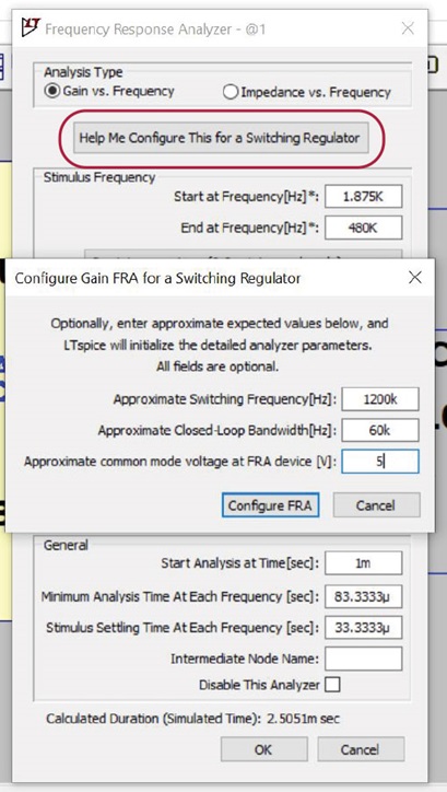
图2. 频率响应分析仪窗口中的波特图设置。
输入开关稳压器的直流输出电压、开关频率和预期稳压器带宽(0 dB交越频率)。完成这些设置之后,按下仿真键。
图3显示了波特图窗口,该窗口会在仿真过程结束后自动打开。在波特图中,频率表示0 dB交越点处的控制回路带宽。在示例中,大约是23 kHz。控制回路的稳定性可通过相位裕度进行评估。相位裕度是指控制回路在0 dB增益交越频率处的相移,图3中标记为“gain_1”。相位裕度应该大于45°,示例中大约为53°,表明该开关稳压器具备足够的稳定性。
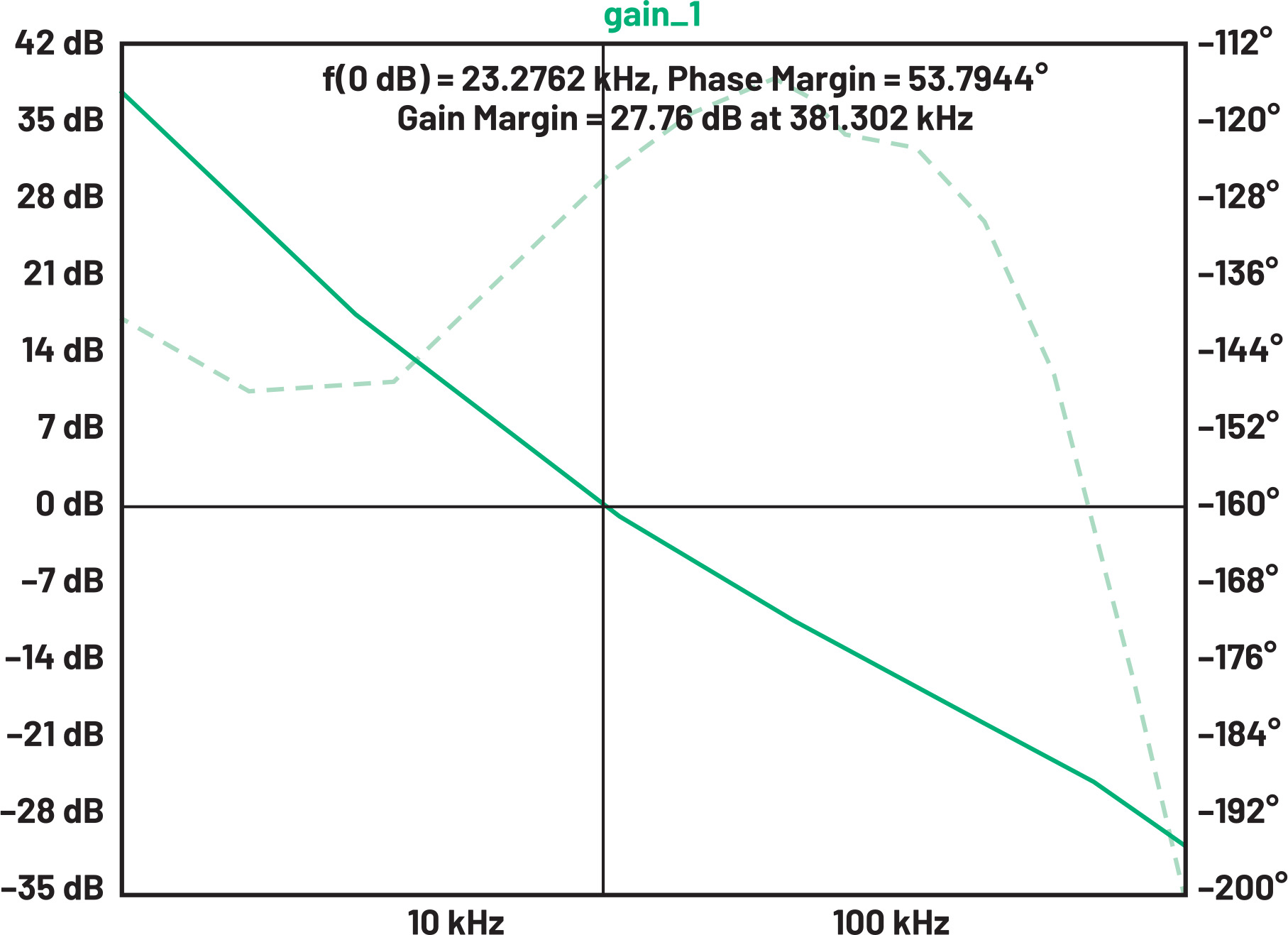
图3. 使用LTspice版本17.1为开关稳压器生成的波特图。
结论
使用LTspice 17.1及更高版本时,FRA模块可使波特图的创建过程变得格外轻松。不仅如此,仿真计算过程得以优化,使得仿真耗时大幅缩短,进而让开关稳压器控制回路优化变得轻而易举。
关于作者
最新视频 21


