摘要
Some IO-Link transceivers (like the MAX22515) can be used to operate as an IO-Link master transceiver with minimal additional components. This application note suggests different circuits to implement the 5mA current sink required in an IO-Link Master and compares their characteristics.
Introduction
An IO-Link master driver must be capable of sinking/sourcing more current than an IO-Link device driver and must include an extra current sink not required on devices/sensors. Some IO-Link device transceivers, like the MAX22515, can be used to operate as a master transceiver with minimal additional components, simplifying the design for these types of applications (e.g., IO-Link configurators, configurable masters, and configurable devices/sensors).
This application note discusses three simple circuits required to use an IO-Link device transceiver for a master or configurable master/device application with the focus on minimizing the inherent power dissipation.
IO-Link System Overview
The IO-Link Master
An IO-Link system consists of a high-level fieldbus controller (PLC or other type of host), an IO-Link master, and at least one IO-Link sensor or device (Figure 1). The IO-Link master bridges communication between any IO-Link devices and the high-level controller.
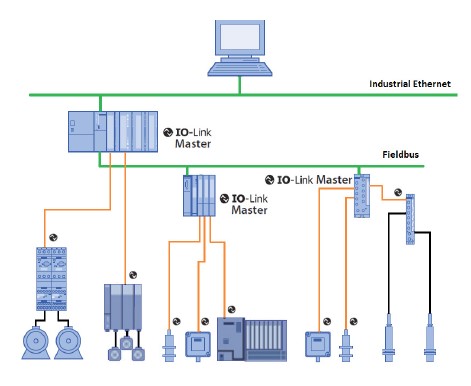
Figure 1. IO-Link system overview.
IO-Link communication is half-duplex and the master initiates all communication with the IO-Link device. Masters and devices are connected in a point-to-point configuration. A master can have many IO-Link master ports and service multiple devices.
An IO-Link master must support any type of device connected to it. The master’s IO-Link C/Q communication line must include a push-pull line driver and a 5mA current sink to discharge the C/Q line when it is not actively driven. The 5mA (min) sink current causes a significant power dissipation in each master power of 5mA x 24V = 120mW at 24V and 150mW at 30V when the C/Q line is driven during the IO-Link data communication. Keeping the sink current as low and close to the 5mA(min) is thus an important goal for the current sink accuracy and tolerance.
Communication between an IO-Link master and a device begins with a wake-up request from the master. To generate a wake-up request, the master driver must be capable of sourcing/sinking at least 500mA for 80µs (typ). An IO-Link master must be able to operate at any of the three IO-Link data rates: COM1 (4.8kbps), COM2 (28.4kbps), and COM3 (230.4kbps) and adapt to the rate of the IO-Link device.
The IO-Link Device
An IO-Link device transceiver is the physical interface between the sensor or actuator’s microcontroller and the IO-Link cable. An IO-Link device line driver may operate as a high-side (PNP) driver or in a push-pull configuration. An IO-Link device communicates at one COM rate only: COM1, COM2, or COM3. The IO-Link device line driver may not push or pull more than 500mA current at any time, ensuring that the master driver dominates control of the line during the master’s IO-Link wake-up pulse.
Configuring an IO-Link Device Transceiver as an IO-Link Master
The MAX22515 IO-Link transceiver is an example of a highly configurable device transceiver that can be used either as a device or master transceiver. Table 1 lists the IO-Link requirements and some of the configurable features of the MAX22515 that allows it to be used as either a device or a master.
| Function | IO-Link Device Requirement | IO-Link Master Requirement | MAX22515 Capability |
| Supply Voltage | 18V to 30V | 20V to 30V | 8V to 36V |
| Driver Configuration | PNP or PP | PNP, NPN, PP | PNP, NPN, PP |
| COM Rate | COM1 or COM2 or COM3 | COM1 or COM2 or COM3 | COM1 or COM2 or COM3 |
| Generate Wake-Up Pulse | No | Yes | Yes |
| Current Sink | No | Yes | Needs External Circuit |
Table 2 shows the required minimum and maximum current sink values listed in the IO-Link specification. The selected component values and voltages need to ensure that these limits are met for IO-Link compliance.
| C/Q Voltage (V) | Min C/Q Current Sink (mA) | Max C/Q Current Sink (mA) |
| 0V to 5V | 0 | 15 |
| 5V to 15V | 5 | 15 |
| 15V to 30V | 5 | 15 |
Because an IO-Link master must include a 5mA current sink, external circuitry is required to use the MAX22515 as a master transceiver. The 5mA (min) sink current is required for a C/Q voltage of higher than 5V (Table 2). A simple 5V/5mA = 1kΩ resistor cannot be used for this purpose, as a 1kΩ resistor results in currents exceeding the 15mA (max) limit at high voltages. For example, when the C/Q voltage is 30V, a 1kΩ resistor would results in a 30mA current sink on the line.
A current sink circuit must be employed. A unity gain current buffer can be conveniently used to realize a high impedance current sink. This application note shows three current buffer circuit implementations and illustrates their characteristics.
Figure 2 shows a basic current-sink circuit that can be added to an IO-Link device transceiver. The diode, DSINK, is used for reverse polarity protection of C/Q. The current sink is permanently on during master operation and can be turned off for SIO or device mode operation.
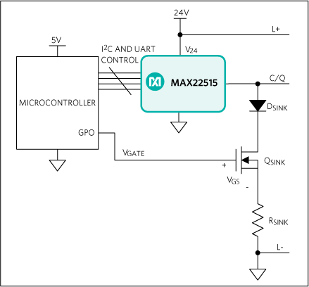
Figure 2. The MAX22515 transceiver configurable as either a master/device using a MOSFET-based current-sink circuit.
Power dissipation in the current sink can be reduced significantly by turning the current sink off dynamically when the master drives the C/Q line high during master data transmission. This can be achieved by driving the transistor’s gate by the UART’s TX output Figure 3.
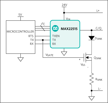
Figure 3. The MAX22515 transceiver with dynamic current-sink circuit.
Selecting the Circuit Components
Selecting the Transistor (QSINK)
Consider the following properties when selecting a MOSFET for the current-sink circuit:
- Drain-to-Source (VDS) voltage rating
- Threshold voltage (VTH)
Select an n-channel MOSFET with a maximum VDS voltage greater than the peak positive voltage expected on the C/Q line, including transient voltages during EMC testing.
To ensure that the MOSFET (QSINK) operates in the saturation region over the required C/Q range (5V = VC/Q = 30V), select an n-channel MOSFET with a small threshold voltage tolerance, since this reduces the variation of the sink current and lowers the typical and worst-case sink currents. Note that various manufacturers of the same transistor part number may specify very different threshold voltages.
Selecting the Diode (DSINK)
Select a diode with a reverse breakdown voltage that exceeds the maximum voltage expected on the C/Q line, including EMC testing.
Selecting the Sink Current Resistor (RSINK)
The RSINK resistor value and the voltage across it are the primary determinants (Ohms law) of the sink current, ISINK. Since a MOSFET draws no DC gate current, its source current equals its drain current (=ISINK). Hence:
ISINK = (VDRIVE - VTH)/RSINK
where VDRIVE is the MOSFET’s gate drive voltage and VTH is the threshold voltage of the QSINK MOSFET.
The 5mA (min) current must be ensured under the worst-case (max and min) component tolerance combinations. A typical MOSFET’s VTH tolerance is relatively large in relation to the gate drive voltage (3.3V or 5V). So, its contribution to the possible variation of ISINK is significant. Use a high gate-drive voltage, VDRIVE, relative to the threshold voltage tolerance range to reduce ISINK variation.
Use the following equation to calculate the required RSINK value under worst-case conditions, assuming a ±1% resistor for RSINK:
RSINK ≤ (VDRIVE(MIN) - VTH(MAX))/5mA
Once a standard RSINK value is selected, check the minimum and maximum resulting currents using the following equations:
ISINK(MIN) = (VDRIVE(MIN) - VTH(MAX))/RSINK(MAX)
ISINK(MAX) = (VDRIVE(MAX) - VTH(MIN))/RSINK(MIN)
Where RSINK(MAX) and RSINK(MIN) represent the maximum and minimum resistor tolerance values, typically ±1%.
A Quick Example
Let us look at a quick example using the circuit shown in Figure 1 and the components (Table 3), assuming a 5V (±10%) VDRIVE voltage on the gate of the QSINK transistor. Note that the minimum sink current, QSINK transistor. Note that the minimum sink current, (ISINK(MIN)) is 5mA, (Table 2).
| Component | Part | Manufacturer | Footprint |
| DSINK | CMHSH5-4 | Central Semiconductor Corp. | SOD-123 (1.4mm x 3.6mm) |
| QSINK | BSS138W | On Semiconductor | SOT-323 (2.00mm x 1.25mm) |
The MOSFET datasheet shows the minimum threshold voltage for the BSS138W as 0.8V and the maximum threshold is 1.5V at ID = 1mA. To guarantee the 5mA (min) specified current, use the following equation to include component tolerance effects:
RSINK(MAX) = (VDRIVE (MIN) - VTH(MAX))/ISINK(MIN)
RSINK(MAX) = (4.5V - 1.5V)/5mA = 600Ω
The nearest E96 standard resistor value is 590Ω. Using this value, verify the resulting typical, minimum and maximum current sink values:
ISINK(MIN) = (4.5V - 1.5V)/590Ω = 5.08mA
ISINK(MAX) = (5.5V - 0.8V)/590Ω = 7.96mA
ISINK(typ) = (5.0V - 1.3V)/590Ω = 6.27mA
The calculated 6.27mA typical and 7.96mA maximum currents highlight that, incorporating system and component tolerances, this circuit results in a significantly higher current than the 5mA (min) target. The consequential power dissipation (Pd = VC/Q x ISINK) in the current-sink circuit is 25.4% higher than the 5mA required sink current for the typical case and 58% in the worst case. Using BSS138W MOSFETS from other suppliers that have wider threshold voltage tolerances would result in increased currents and power dissipation.
Note that tighter VDRIVE voltage tolerances, for example ±5%, lead to significantly lower maximum and typical sink currents.
Using these component values and the BSS138W On-Semiconductor MOSFET, the measured currents for the entire C/Q operating range (-30V to 30V) with a gate drive voltage of 5V is shown in Figure 4. The measured values shown in Figure 4 show a noticeable increase in output current with C/Q voltage due to the MOSFET’s output conductance: At a C/Q voltage of 5V, the sink current is 6.11mA and it increases to 6.42mA when C/Q is 30V. This is a 5% increase in current and, subsequently, in elevated power dissipation at 30V due to output conductance.
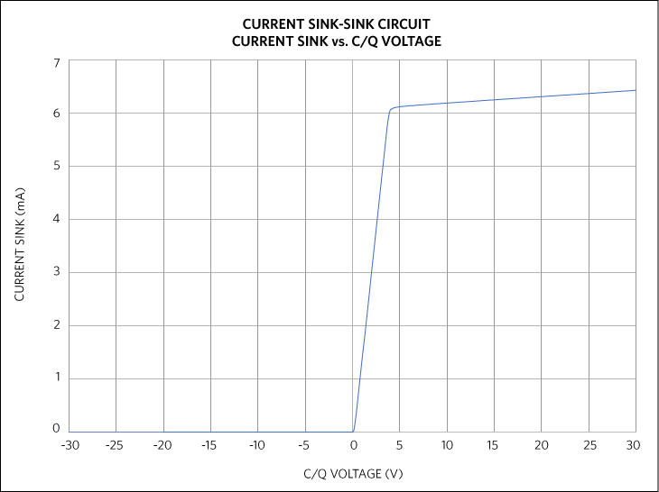
Figure 4. BSS138W current-sink circuit measurements vs. C/Q voltage.
BJT vs. MOSFET in Current-Sink Circuit
A bipolar transistor can be employed to reduce the power dissipation, compared to a MOSFET-based solution, as the VBE voltage variation is typically much smaller than a general MOSFET's threshold tolerance range. Additionally, for applications with the drive voltage less than 5V, an NPN transistor must be used in place of a MOSFET (QSINK) (Figure 5) due to the lower VBE tolerance relative to the lower VDRIVE voltage.
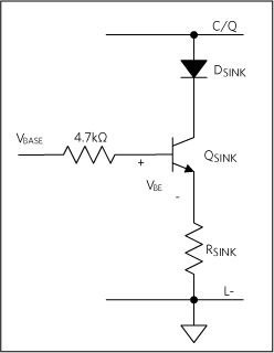
Figure 5. External sink current circuit using an NPN transistor.
The BJT-based circuit requires a series base resistor to reduce the high BJT base current of ~5mA when the C/Q voltage is low or during C/Q reverse polarity conditions.
The following equation defines the emitter current, which is close (<1%) to the collector current (ISINK) when using a high (>100) current gain (hFE ) bipolar transistor:
ISINK(MIN) = (VDRIVE - VBE - ISINK x RBASE/ hFE)/RSINK
Rewriting for clarification:
ISINK = (VDRIVE - VBE)/RSINK + RBASE/hFE)
Let us look at a quick example using the BC846BM3T5G from On-Semiconductor. According to the BC846BM3T5G datasheet, the minimum base-emitter voltage VBE(on) of the transistor is 580mV at IC = 2mA, and the maximum is 700mV. The minimum hFE is 200 and maximum is 450. Let us start by assuming a 4.7kO base resistor, resulting in a 5.5V/4.7kΩ = 1.1mA base current when the C/Q voltage is low. Using these values, the RSINK value is:
RSINK(MAX) = (VDRIVE(MIN) - VBE(ON)(MAX) - RBASE x /ISINK(MIN)/ hFE(MIN)) / ISINK(MIN)
RSINK(MAX) = (4.5V - 0.70V – 4.7kΩ x 5mA /200) / 5mA = 736.5Ω
The nearest E96 standard resistor value is 732Ω.
Calculate the resulting typical, minimum and maximum sink currents:
ISINK(MIN) = (4.5V - 0.70V)/732Ω + 4.7kΩ/200) = 5.03mA
ISINK(MAX) = (5.5V - 0.58V)/732Ω + 4.7kΩ/450) = 6.63mA
ISINK(typ) = (5.5V - 0.66V)/732Ω + 4.7kΩ/450) = 5.80mA
This BJT solution shows a 16% (typ) and 33%(max) higher current than the 5mA required minimum current shown in Table 2. This is a significant improvement over the MOSFET-based circuit and the increased power dissipation of the BJT circuit is only about half of the MOSFET circuit.
Calculate the base currents for the BJT circuit to check if it is within the VDRIVE driver’s capability and if the power dissipation in the VDRIVE circuit is acceptably low. The selected base resistor value of 4.7kΩ results in a worst-case base current of (5.5V - 0.58V)/(732Ω + 4.7kΩ) = 0.9mA (max) when C/Q is low. When C/Q is high, the base current is 5.80mA / 290 = 20µA (typ). These base current levels should be acceptable for most applications.
Using these components and the BC846BM3T5G NPN transistor, the measured currents for the entire C/Q operating range (-30V to 30V) with a VDRIVE voltage of 5.0V is shown in Figure 6. The measurements show 5.73mA current at 5V and 5.92mA at 30V, which is a 3.3% increase in current due to the output conductance resulting from the BJT’s Early voltage. This output conductance is lower than the BJT circuit tested previously.
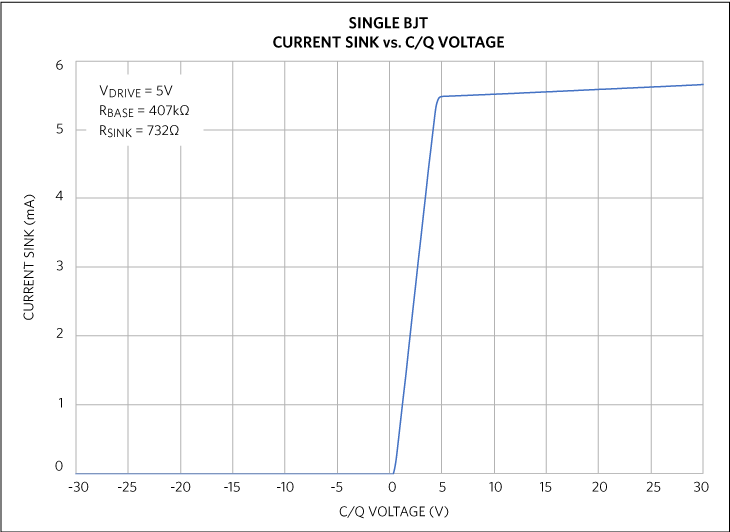
Figure 6. Single NPN BJT transistorncurrent-sink circuit measurements vs. C/Q voltage.
Further Reducing Power Dissipation with a Cascode Configuration
The current measurements for the circuits in Figure 2 (MOSFET current-sink) and Figure 5 (single BTJ current-sink) highlight that these circuits have significant output conductance that results in a 5% or 3.3% rise in current as the C/Q voltage increases from 5V to 30V. To reduce this rise in current and minimize the resulting power dissipation at high C/Q voltages, a cascode configuration can be utilized in place of a single MOSFET or BJT, at the cost of a slight increase in the circuit footprint. A cascode configuration keeps the collector-emitter voltage of the current determining transistor constant and independent of C/Q voltage changes. Figure 7 shows a current-sink circuit using the MAX22515 and two BC846BM3T5G NPN BJT transistors in a cascode configuration.
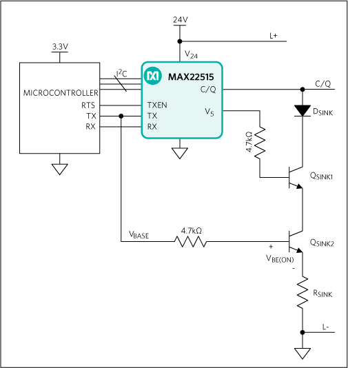
Figure 7. NPN-based cascode current-sink circuit.
Note that a cascode configuration could also be configured with two n-channel MOSFETs or one NPN transistor (QSINK1) and one n-channel MOSFET (QSINK2).
Assuming 3.3V ±10% drive on the lower NPN (VDRIVE2) and 5V ±10% drive on the top transistor (VDRIVE1), the component calculations are analogous to the single BJT circuit. Using the BC846BM3T5G the calculation is:
RSINK(MAX) = (VDRIVE(MIN) - VBE(ON)(MAX) - RBASE x ISINK(MIN)/hFE(MIN))/ISINK(MIN)
RSINK(MAX) = (3.0V - 0.70kΩ x 5mA/200)/5mA = 436.5Ω
The nearest E96 standard resistor value is 432Ω. Using this value, the minimum, typical and maximum resulting currents are calculated as:
ISINK(MIN) = (3.0V - 0.70V)/(432Ω + 4.7kΩ/200) = 5.05mA
ISINK(MAX) = (3.6V - 0.58V)/(432Ω + 4.7kΩ/450) = 6.83mA
ISINK(MAX) = (3.3V - 0.66V)/(432Ω + 4.7kΩ/290) = 5.89mA
This cascode solution thus has a 18% (typ) and 37%(max) higher current than the 5mA required minimum. This is minimally higher that the single BJT circuit, due to the 3.3V±10% VDRIVE but significantly lower than the single MOSFET circuit.
Figure 8 shows the measurements with a VDRIVE1 = 5V and VDRIVE2 = 3.3V base drive voltage, using the configuration shown in Figure 7 and the BC846BM3T6G transistors. With a 3.3V gate voltage, the measured sink current is 5.739mA at VC/Q = 5V and a maximum current sink of 5.779mA at VC/Q = 30V. The 40µA current increase between a C/Q voltage of 5V and 30V represents a 0.7% increase due to output conductance. This results in a negligible power dissipation increase over the entire C/Q voltage range due to the cascode’s very low output conductance.
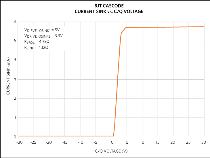
Figure 8. Cascode current-sink circuit measurements vs. C/Q voltage.
Conclusion
Some IO-Link device transceivers can operate as both IO-Link device or/and IO-Link master transceivers with the addition of only a few circuit components. The MAX22515 IO-Link device transceiver is an example of a highly configurable transceiver that can be used in either configuration with the addition of a current sink circuit. The application note discusses the use of three simple current sink circuits with their performance overview summarized in Tables 4 and 5. The MOSFET-based current sink is the least attractive as it has the highest output currents, primarily due to a MOSFET’s large threshold voltage tolerance.
The cascode configuration shows the lowest output conductance resulting in lowest power dissipation overhead at high C/Q voltages. The single BJT current sink, when driven by 5V±5%, represents the lowest power solution, and outperforms the cascode variant with the lowest power dissipation
| Circuit Configuration | VDRIVE Range | Calulated Sink Current | Maximum Current-Sink/5.0mA Ratio | |||
| Typ | Max | |||||
| Single MOSFET (Figure 2) | 5V±10% | 6.27mA | 7.96mA | 60% | ||
| Single BJT (Figure 5) | 5V±10% | 5.80mA | 6.63mA | 33% | ||
| Single BJT (Figure 5) | 5V±5% | 5.53mA | 6.00mA | 20% | ||
| Single BJT (Figure 5) | 3.3V±10% | 5.89mA | 6.83mA | 37% | ||
| Cascode - BJT (Figure 7) | 3.3V±10% | 5.89mA | 6.83mA | 37% | ||
| *Calculated values are with respect to the power dissipation expected with a current sink value of 5.0mA. | ||||||
| Circuit Configuration | Measure Sink Current | Increase In Current (5V ≤ C/Q ≤ 30V) | Conductance-Related Power Dissipation AT C/Q = 30V | |
| C/Q = 5V | C/Q = 30V | |||
| Single Mosfet (Figure 2) | 6.11mA | 6.42mA | 310µA | 9.3mW |
| Single BJT (Figure 5) | 5.742mA | 5.919mA | 177µA | 5.3mW |
| Cascode - BJT (Figure 7) | 5.739mA | 5.779mA | 40µA | 1.2mW |
最新视频 21


