摘要
CMOS source followers are not easy circuits to design, but by careful analysis and by taking source resistance into account in the BSIM models, designers can achieve more accurate results to achieve better matching in the design of low-noise amplifiers.
Introduction
The CMOS source follower is a difficult device to design using a CMOS device, because the transconductance of a CMOS device is low compared to that of a bipolar junction transistor (BJT). Thus, nonconventional followers must be designed to give a gain close to 1. In comparison, the gain of a simple common-drain follower is much less than 1. However, after analysis, you can see that not only transconductance affects the gain of the amplifier—with shrinking semiconductor processes and smaller devices, the source resistance (RS) also contributes to reduced gain.
Measurement of Gain
The circuit in Figure 1 shows a simple common-drain amplifier used to measure gain.
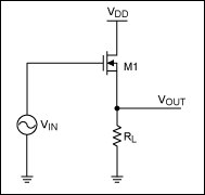
Figure 1. Test circuit for gain measurements.
Figure 2 shows a small-signal model that can be drawn from the Figure 1 circuit.
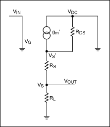
Figure 2. Small-signal model of the Figure 1 circuit.
From Figure 2, it can be shown that the gain (G) of a simple common-drain follower is:

Where gL is transimpedance of the load (RL), gDS is transimpedance of the drain-source resistance (RDS) of the CMOS device, and gm is CMOS transconductance.
Using a TSMC 0.18µm process with a CMOS device (the Figure 1 nFET, M1) having a width of 5µm and a length of 0.18µm, the expected gain and measured gain were obtained for a 100mV AC waveform at 10kHz (see Table 1).
| VG(DC) (V) | Expected Gain | Measured Gain |
| 1.2 | 0.836 | 0.655 |
| 1.0 | 0.7490 | 0.63 |
| 0.9 | 0.703 | 0.612 |
| 0.75 | 0.631 | 0.56 |
The Table 1 results show that there is an additional loss in gain, which is caused by RS.
Calculating Source Resistance (RS)
Figure 3 shows the circuit that results from calculating a DC solution for the Figure 2 small-signal model.
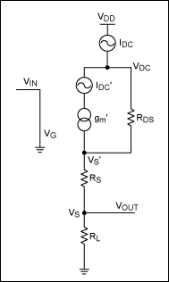
Figure 3. A DC model of the simple common-drain follower.
The following parameters can be extracted from a simulation using the Figure 3 model:
- IDC: measured DC current
- VS: voltage of the source
- VIN: AC input voltage (100mV) at 10kHz
- VDD: supply voltage
- RDS: drain-source resistance
From these, you can then calculate the intrinsic gm' by using:

Where IDC' is simply:

and:

Assuming that:

and:
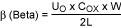
Where β is the DC gain from the transistor, UO is surface mobility, COX is gate oxide capacitance per unit area, W is transistor gate width, and L is transistor gate length.
Note: The intrinsic gm' can only be measured using the measured DC current, because VGS' cannot be measured without RS.
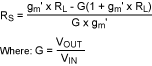
Using the Figure 2 small-signal model, the following measured gain equation can be derived. This equation takes into account the effects of gm' by RDS, as previously described.
Measuring Source Resistance (RS)
The RS results in Table 2 were obtained using the same transistor that was used for the gain measurements (width = 5µm, length = 0.18µm, input AC waveform of 100mV at 10kHz).
| VG(DC) (V) | IDC (µA) | gm' (mA/V) | RS (Ω) |
| 1.2 | 364 | 2.75 | 370 |
| 1.0 | 251 | 2.26 | 357 |
| 0.9 | 197 | 1.99 | 357 |
| 0.75 | 119 | 1.52 | 375 |
Conclusion
From the results shown in this article, it can be seen that RS is a valid concern and has a major effect on the gain of a source follower. The results show a 5% spread in the value of RS, which is probably due to the estimates of the value of RDS when simulated. It is also worth mentioning that the value of RS affects the value of the calculated transconductance—this is because transconductance is currently calculated using the measured VGS value, which includes a voltage drop across RS that is assumed to be negligible in value. However, because RS is real and there is a valid voltage drop across the source resistance, the transistor's VGS is effectively reduced, which in turn reduces the transconductance of the CMOS device.
Using a transistor of a 5µm to 10µm width, one would expect RS to be reduced by half. However, this was not the case, and the resulting measurements highlighted that the resistances were similar in value. After further investigation, it was found that the design kit that was used based its calculations on a minimum source area. Without the addition of BSIM parameters to the transistor model, RS is inaccurately calculated and simulated in the majority of cases. This means that there is always a mismatch between real silicon and simulations when calculating measurements such as transistor transconductance. This is already taken into account with RF designs, such as the MAX2645 low-noise amplifier, in which matching is essential to prevent loss due to insertion and voltage-wave reflection. This concern can be overlooked in baseband designs, which use standard design kits.
A similar article appeared in the March 2008 issue of Chip Design Magazine.
关联至此文章
产品
产品分类
{{modalTitle}}
{{modalDescription}}
{{dropdownTitle}}
- {{defaultSelectedText}} {{#each projectNames}}
- {{name}} {{/each}} {{#if newProjectText}}
-
 {{newProjectText}}
{{/if}}
{{newProjectText}}
{{/if}}
{{newProjectTitle}}
{{projectNameErrorText}}
最新视频 20