摘要
本文比较了MAXQ与其它微控制器竞争产品的指令系统,包括PIC16CXXX (中档器件)、AVR和MSP430。并以表格方式列出了各种指令系统的优势和弱点。我们将利用选定的算法和操作程序判断不同系统的代码密度和代码性能,最后一节重点介绍各例程的MIPS (每秒百万条指令)/mA比率。
Overview of MAXQ Instruction Set
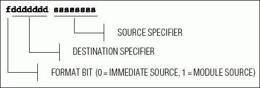
The MAXQ instruction set is founded upon the transfer-trigger concept. The instruction word is composed simply of source and destination operands. While these source and destination operands may represent physical registers, the encodings may also represent indirect access points to data memory, stack memory, and the working accumulators, and/or may implicitly trigger hardware operations. Additional information on the MAXQ transfer-triggered architecture can be found in application note 3222, "Introduction to the MAXQ Architecture." Source and destination encodings for specific MAXQ devices are defined in the MAXQ User Guide(s) associated with the device. While some source and destination encodings may be device specific, such as those designated for peripheral hardware functions, certain fixed encodings are identified for building the MAXQ base instruction set. Figure 1 gives the MAXQ instruction word and instruction set mnemonics.
| MNEMONIC | DESCRIPTION | MNEMONIC | DESCRIPTION |
| BIT MANIPULATION | LOGICAL | ||
| MOVE C, #0/#1 | Clear/Set Carry | AND | Logical AND |
| CPL C | Complement Carry | OR | Logical OR |
| AND Acc.<b> | Logical AND Carry with Accumulator Bit | XOR | Logical XOR |
| OR Acc.<b> | Logical OR Carry with Accumulator Bit | CPL, NEG | One's, Two's Complement |
| XOR Acc.<b> | Logical XOR Carry with Accumulator Bit | SLA, SLA2, SLA4 | Shift Left Arithmetically 1,2,4 |
| MOVE C, Acc.<b> | Move Accumulator Bit to Carry | SRA, SRA2, SRA4 | Shift Right Arithmetically 1,2,4 |
| MOVE Acc.<b>,C | Move Carry to Accumulator Bit | SR | Logical Shift Right |
| MOVE C, src.<b> | Move Register Bit to Carry | RR, RRC | Rotate Right Carry (Ex/In)clusive |
| MOVE dst.<b>, #0/#1 | Clear/Set Register Bit | RL, RLC | Rotate Left Carry (Ex/In)clusive |
| MATH | DATA TRANSFER | ||
| ADD, ADDC | Add Carry (Ex/In)clusive | XCHN | Exchange Accumulator data nibbles |
| SUB, SUBB | Subtract Carry (Ex/In)clusive | XCH (MAXQ20) | Exchange Accumulator data bytes |
| FLOW CONTROL AND BRANCHING | MOVE dst, src | Move source to destination | |
| JUMP {C/NC/Z/NZ/E/NE/S} | Jumps - unconditional or conditional, relative or absolute | PUSH/POP | Push/Pop stack |
| DJNZ LC[n], src | Decrement Counter, Jump Not Zero | POPI | Pop stack and enable interrupts (INS<0) |
| CALL | Call - relative or absolute | Other | |
| RET {C/NC/Z/NZ/S} | Return - unconditional or conditional | NOP | No Operation |
| RETI {C/NC/Z/NZ/S} | Return from Interrupt - unconditional or conditional | CMP | Compare with Accumulator |
Figure 1. The source-to destination transfer illustrated in the MAXQ instruction word produces a small, yet very potent instruction set.
| ISA | STRENGTH | WEAKNESS |
| AVR |
|
|
| PIC16CXXX |
|
|
MAXQ vs. Other Instruction-Set Architectures
One could attempt to compare the MAXQ instruction mnemonics against those of other architectures, but this analysis would be difficult and unjustified because each instruction set is architected around specific device resources and addressing modes. For this reason, the instruction set and the device architecture (instruction cycle, memory model, register set, addressing modes, etc.) are inseparable and must be considered together. Table 1 summarizes the strengths and weaknesses of the instruction-set architectures being compared.
Code Examples
The best way to compare instruction-set architectures is to define some set of tasks and write the code to perform those tasks. The sections that follow describe certain tasks to be performed and summarize the code density and performance results for each instruction-set architecture. Example code for the first routine is included in the document, while the routines that follow will only be summarized with graphs and text. The code routines corresponding to each set of statistics are available from Maxim upon request.
| ISA | STRENGTH | WEAKNESS |
| MSP430 |
|
|
| MAXQ |
|
|
Memory Copy (MemCpy64)
The memory copy example demonstrates the microcontroller's ability to indirectly manipulate blocks of data memory. The task is to copy 64 bytes from a data-memory source location to a nonoverlapping data-memory destination. The code routines for each microcontroller are provided on the following pages, along with graphs that summarize the cycle count and byte count for the copy operation. These routines assume that the pointer and byte count have already been defined before the copy operation, and that the bytes to be copied are word-aligned in memory so the word access modes of the MSP430 and MAXQ20 can be used.
;======================================AVR======================================
; ramsize=r16       ;size of block to be copied
; Z-pointer=r30:r31     ;src pointer
; Y-pointer=r28:r29     ;dst pointer
; USES:
; ramtemp=r1      ;temporary storage register
loop:           ; cycles
  ld ramtemp,Z+       ; 2 @src => temp
  st Y+,ramtemp       ; 2 temp => @dst
  dec ramsize       ; 1
  brne loop       ; 2/1
  ret         ; 4/5
          ;---------
          ;(7*bytecount) + return - 1(last brne isn't taken).
; WORD COUNT = 5 ; CYCLE COUNT = 451>

;=====================================MAXQ10====================================
; DP[0] ; src pointer (default WBS0=0)
; DP[1] ; (dst-1) pointer (default WBS1=0)
; LC[0] ; byte count (Loop Counter)
loop:         ;words & cycles
  move DP[0], DP[0]     ; 1 implicit DP[0] pointer selection
  move @++DP[1],@DP[0]++  ; 1
  djnz LC[0], loop    ; 1
  ret       ; 1
        ;----------
        ; 4 / (3*bytecount) +1
; WORD COUNT = 4 ; CYCLE COUNT = 193

;====================================MAXQ20=====================================
; Assuming bytes are word aligned (like MSP430 code) for comparison
; DP[0] ; src pointer (default WBS0=1)
; DP[1] ; (dst-1) pointer (default WBS1=1)
; LC[0] ; byte count / 2 (Loop Counter)
loop:       ;words/cycles
  move DP[0], DP[0]     ; 1 implicit DP[0] pointer selection
  move @++DP[1],@DP[0]++  ; 1
  djnz LC[0], loop    ; 1
  ret       ; 1
        ;----------
        ; 4 / (3*bytecount/2) +1
; WORD COUNT = 4 ; CYCLE COUNT = 97

;====================================MSP430=====================================
; MSP430 has a 16-bit data bus
; assuming bytes are word aligned, only requires (blocksize/2 transfers).
; R4  ;src pointer
; R5  ;dst pointer
; R6  ;size of block to copy
loop:         ;words/cycles
  mov @R4+, 0(R5)     ;2 / 5 @src++ => dst
  add #2, R5    ;1 / 1 const generator makes this 1/1
  decd.b R6     ;1 / 1 really sub #2, R6
  jz loop       ;1 / 2
  ret       ;1 / 3
        ;----------
        ;6 / (9*(bytecount/2)) + return
; WORD COUNT = 6 ; CYCLE COUNT = 291

;===================================PIC16CXXX===================================
; a   ; src pointer base
; b   ; dst pointer base
; i   ; byte count held in reg file
; USES:
; temp  ; temp data storage
loop:         ; cycles
  decf i, W     ; 1 i-- => W
  addlw a       ; 1 (a+i--) => W starting at end
  movwf FSR     ; 1 W => FSR
  movfw INDF    ; 1 W <= @FSR get data
  movwf temp    ; 1 W => temp
  movlw (b-a)     ; 1 diff in dest-src
  addwf FSR, F    ; 1 (b+i--) => W
  movfw temp    ; 1 temp => W
  movwf INDF    ; 1 W => @FSR store data
  decfsz i, F     ; 2/1 i--
  goto loop     ; 2
  return      ; 2
        ;----------
        ;11 / (12*bytecount) +1 (ret instead of goto, +1 on decfsz)
; WORD COUNT = 12 ; CYCLE COUNT = 769 (*4clks/inst cycle = 3076)
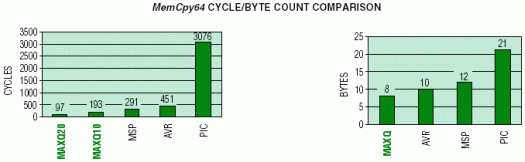
The MAXQ devices provide the best code density and are the clear winners in execution speed. The MAXQ10 performs the copy operation slower than the MAXQ20 because it uses the default byte-access mode for the data pointers. For a MAXQ10 application, if execution speed is deemed more important than code density and the data memory to be copied is word-aligned (an assumption already being made for the MSP430 and MAXQ20 example), it could use wordaccess mode for the source and destination data pointers. Enabling word mode would allow the MAXQ10 copy loop to be cut in half, but would require additional instructions to enable/disable word-access mode. The overwhelming performance advantage demonstrated by the MAXQ devices over the competition can be attributed to the following architectural strengths:
| 1. | No pipelining - branches do not incur the overhead of flushing the instruction prefetch as other devices do. |
| 2. | Auto-decrement loop counter - alleviates the need to do this manually. |
| 3. | Harvard memory map - program and data do not share the same physical space, allowing simultaneous program fetch and data access. |
| 4. | Pre-increment/decrement indirect destination pointer - simplifies and speeds advancement of the destination pointer. This is a weakness of the MSP430, which uses 0(R5) to denote @R5, and then must advance that destination pointer using another instruction. |
The MAXQ advantages illustrated in the memory copy example translate into similar gains for applications requiring frequent input/output buffering in data memory. In terms of performance, the nearest competitor is the MSP430. As an example where data memory buffering may be desired, suppose we have an MSP430 device equipped with an ADC peripheral with a 16-bit output register. Transferring data from the peripheral output register into data memory and incrementing the pointer in preparation for the next ADC output sample might be handled with code such as this:
                                                ; words/cycles
      mov.w       &ADAT,0(R14)                  ; 3 / 6              Store output word
                    incd.w R14                  ; 1 / 1              Increment pointer
                                                ; 4 / 7
The same transfer operation would look like this on the MAXQ20:
move @++DP[0], ADCOUT ; 1 / 1
Bubble Sort (BubbleSort)
The bubble sort routine not only demonstrates the ability to access data memory efficiently, but also performs arithmetic and/or comparison operations between data bytes and conditionally reorders the bytes. The code routine sorts 32 data-memory bytes so they are left in an ascending or descending order. The cycle counts assume that byte reordering occurs approximately half of the time as a result of adjacent byte comparisons. The graphs below summarize the cycle count and byte count for the sort operation on each microcontroller.
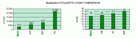
The MAXQ devices, once again, yield the best code density and are the clear winners in execution speed. The MAXQ advantages can be attributed to the same architectural strengths discussed in the memory copy example.
Hex-to-ASCII Conversion (Hex2Asc)
This conversion routine tests the scope of the microcontrollers' arithmetic and logical operations. It also tests their support of literal byte data when translating and expanding data contained within a single byte. The cycle count represents an average value, given that each nibble can be one of 16 hex values - 0 to 9, Ato F. The graphs below summarize the cycle count and byte count for the conversion operation on each microcontroller.
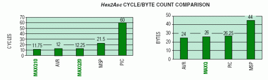
For this test routine, the AVR requires one fewer word since its working registers are directly accessible, whereas the most efficient method for the MAXQ requires a manual update of the accumulator pointer. The MSP code density suffers because it lacks operations for manipulating nibbles, and because literals (#nnnnh) not supported by the constant generator must be encoded in a separate word. The MAXQ devices and the Atmel AVR achieve similar results in the performance area, while other devices lag behind. The MSP430 performance suffers from the extra code words to perform the operation.
Arithmetic Shift Right 2 Positions (ShRight)
This routine demonstrates the microcontrollers' ability to support 16-bit word data-memory access and ALU operations. The desired operation is to arithmetically shift (i.e., preserving the most significant bit) a 16-bit word that resides in data memory. It is assumed that the word resides in the first 256 bytes of data memory and is aligned in memory to be word addressable by those microcontrollers with the capability. The following graphs summarize the cycle count and byte count for the shift operation on each microcontroller.
Both microcontrollers that support 16-bit ALU operations, the MAXQ20 and MSP430, provide significantly better code density. With exception of the PIC, all of the 8-bit machines require at least twice the number of code words to accomplish the same arithmetic shift. The MAXQ20 offers the best performance, and the MAXQ10, while supporting only 8-bit ALU operations, approaches the performance of the 16-bit MSP430.
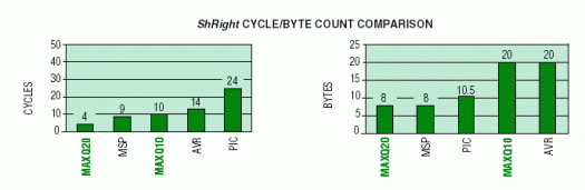
The MAXQ20 and MSP430 demonstrate higher ode density because of their ability to handle 16-bit data more efficiently than the 8-bit machines. Each does so, however, in a slightly different fashion. The MAXQ20 transfers the 16-bit word to be shifted into a working register (accumulator) where it can use a multibit arithmetic shift. The MSP430 performs single-bit arithmetic shift operations using the register indirect-addressing mode (RRA @R5), and does not explicitly transfer the word from its memory location. While offering higher performance, the MAXQ20 can provide the same or better code density as the MSP430, when the arithmetic shifting of a 16-bit word can use one of the multibit arithmetic shift op codes (SRA2, SRA4, SLA2, SLA4).
Bit-Bang Port Pins (BitBang)
This example tests the ability of an instruction-set architecture to decompose bytes, either by direct bit manipulation or through shift/rotate, and send the individual bits to a port pin ("bitbanging"). The port-pin outputs separately represent clock and data, with the requirement that data must be valid on the rising edge of clock. Since the code is directly manipulating the port pins, this test also demonstrates the ease with which I/O port registers can be accessed. The graphs below summarize the cycle count and byte count for the port bit-bang operation on each microcontroller.
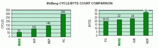
The MAXQ devices again are clearly the best performers. The PIC performance is limited here (as in other examples) because of the underlying 4-cycle core architecture. The MSP430 performance is worse and can be attributed to both its Von Neumann memory architecture and required use of absolute addressing to access the port output register.
With respect to code density, the MAXQ and PIC have the same word count. Yet the PIC edges out the MAXQ among the RISC machines because of its 14-bit program word versus the 16-bit program word of the MAXQ. The MSP430 code density suffers because it must use at least two words to access its peripheral registers with the absolute-addressing mode (i.e., & register) or when using literals that cannot be reduced by the constant generator (e.g., #3h).
The MSP430 method of accessing its peripheral registers deserves further comment. The microcontroller's primary duty is to interface in some way with the outside world. Thus it must control, monitor, and process activity that occurs at I/O pins. If the microcontroller embeds very few peripheral-hardware modules, the burden of this activity is left to the software. For the software to do anything meaningful, it must read and write the port pins. On the MSP430, these port-pin registers reside in the peripheral register space that requires use of the absolute-access mode. Now consider a microcontroller that is rich with "smart" peripherals. There will undoubtedly be more peripheral registers that must be configured, controlled, and accessed during the course of using the on-chip, dedicated hardware to perform the necessary function. On the MSP430, these registers reside in the peripheral register space that requires use of the absolute-access mode. Consequently, there is no escape around the code density and performance penalty associated with the MSP430 absolute addressing mode.
The "MIPS/mA" Metric
Power consumption is often a significant factor in the selection of a processor or core architecture. The overall power consumption of a given system depends upon many factors such as supply voltage and operating frequency, and its ability to use low-power modes whenever possible. Reduced supply voltage(s) and/or operating frequency, along with frequent use of low-power modes, can greatly reduce the total system power consumption. While the minimum supply voltage for a given microcontroller depends greatly upon the device fabrication process technology, the ability to reduce operating frequency and use low-power mode(s) is largely dependent upon application requirements that can be determined by the system designer. The MIPS/mA metric provides a simple means for assessing the code efficiency of a microcontroller while factoring in active current consumption. A common supply voltage should be chosen to create meaningful MIPS/mA comparisons between different devices. For the forthcoming comparison, a 3V-supply voltage is assumed. To factor in differences and efficiencies in the instruction-set architectures being compared (i.e., AVR, MSP430, PIC16, MAXQ), it is also necessary to generate separate MIPS/mA ratios for each code example generated.
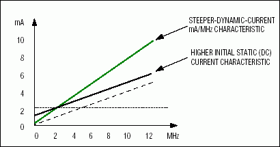
Figure 2. This example for IccActive vs. MHz illustrates the effects of increased static and dynamic current.
To determine the "mA" portion of the MIPS/mA ratio, we examine data sheets of the devices. Most microcontroller vendors specify typical and maximum active current associated with the maximum operating frequency of the device. Assuming very small static (DC) current, these data points allow one to derive typical and maximum mA/MHz approximations used for extrapolating active current at any clock frequency. The mA/MHz ratio can be better quantified and defined relative to specific system environmental conditions if the vendor provides active current vs. temperature/frequency characterization data. Otherwise, we must simply rely on the discrete data points and our assumption of very small static current. Increased static (DC) current changes the starting point for the mA vs. MHz characteristic curve, thereby limiting the overall gain seen by the system designer when reducing clock frequency (reducing dynamic current). Figure 2 gives an example IccActive vs. MHz graph. Table 2 compares mA/MHz numbers for the various cores and cites the source for the information. The highlighted mA/MHz number for each architecture is used when this term is required in later calculations.
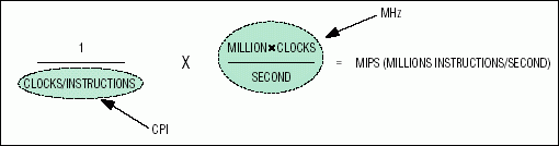
Figure 3. The MAXQ architecture achieves a high-MIPS performance ratio by executing nearly all instructions at one clock per instruction.
The "MIPS" portion of the MIPS/mA metric is used to quantify the difference in performance. We will start by giving a simple equation for MIPS in Figure 3.
The number of clocks per instruction (CPI) is highly important when assessing MIPS for a given architecture. Architectures such as the Microchip PIC, for example, require multiple clocks per instruction cycle. Additionally, architectures often require multiple instruction cycles to execute certain instructions or need cycles to flush the instruction pipeline when performing jumps/branches. When comparing architectures, the average performance in MIPS is often much less than the peak performance (MIPS) and varies depending upon instruction mix.
| DEVICE | TYPICAL mA/MHz | MAX mA/MHz | SOURCE |
| PIC16C55X | 0.7 | 1.25 | PIC16C55X data sheet: DC Table 10.1, D010 (VCC = 3V, 2MHz); XT or RC |
| PIC16C62X | 0.7 | 1.25 | PIC16C62X data sheet: DC Table 12.1, D010 (VCC = 3V, 2MHz); XT or RC |
| PIC16LC71 | 0.35 | 0.625 | PIC16C71X data sheet: DC Table 15.2, D010 (VCC = 3V, 4MHz); XT or RC |
| PIC16F62X | 0.15 | 0.175 | PIC16F62X data sheet: DC Table 17.1, D010 (VCC = 3V, 4MHz) |
| PIC16LF870/1 | 0.15 | 0.5 | PIC16F870/1 data sheet: DC Table 14.1, D010 (VCC = 3V, 4MHz); XT or RC |
| AT90S1200 | 0.33 | 0.75 | AT90S1200 data sheet: EC Table (3V, 4MHz), Figure 38, 4mA/12MHz (typ) |
| AT90S2313 | 0.50 | 0.75 | AT90S2313 data sheet: EC Table (3V, 4MHz), Figure 57, 7.5mA/15MHz (typ) |
| MSP430F1101 | 0.30 | 0.35 | MSP430x11x1 data sheet: DC specs IccActive (VCC = 3V, FMCLK = 1MHz) |
| MPS430C11X1 | 0.24 | 0.30 | MSP430x11x1 data sheet: DC specs IccActive (VCC = 3V, FMCLK = 1MHz) |
| MSP430Fx12x | 0.30 | 0.35 | MSP430x12x data sheet: DC specs (VCC = 3V, FMCLK = 1MHz, FACLK = 32kHz) |
| MAXQ10 | 0.30 | Simulations | |
| MAXQ20 | 0.30 | Simulations |
To produce a more useful indicator and generate a value that helps us reach our MIPS/mA target metric, we divide MIPS by MHz. The MIPS/MHz ratio can be interpreted as the average number of instructions that execute in a single clock (for the given code example). Using the MIPS/MHz number and the mA/MHz number calculated earlier, the MIPS/mA ratio can be generated. The tables below show the MIPS/MHz and MIPS/mA numbers, respectively, for each of the earlier code-routine comparisons.
| CORE | MIPS/MHz | |||||
| MemCpy64 | BubbleSort | Hex2Asc | ShRight | BitBang | Peak | |
| MAXQ10 | 1.00 | 0.99 | 1.00 | 1.00 | 1.00 | 1 |
| MAXQ20 | 1.00 | 0.99 | 1.00 | 1.00 | 1.00 | 1 |
| PIC | 0.23 | 0.20 | 0.23 | 0.25 | 0.21 | 0.25 |
| MSP | 0.44 | 0.39 | 0.64 | 0.33 | 0.61 | 1 |
| AVR | 0.57 | 0.62 | 0.90 | 0.71 | 0.61 | 1 |
| CORE | MIPS/mA | |||||
| MemCpy64 | BubbleSort | Hex2Asc | ShRight | BitBang | ||
| MAXQ10 | 3.33 | 3.30 | 3.33 | 3.33 | 3.33 | |
| MAXQ20 | 3.33 | 3.30 | 3.33 | 3.33 | 3.33 | |
| PIC | 1.53 | 1.35 | 1.53 | 1.67 | 1.40 | |
| MSP | 1.85 | 1.62 | 2.66 | 1.39 | 1.55 | |
| AVR | 1.71 | 1.86 | 2.69 | 2.14 | 1.83 | |
To take the analysis one step further, we must factor in differences between core architecture and instruction-set efficiency by dividing the MIPS/mA ratio by the number of instructions that are actually executed for the given code sample. The rationale for this extra calculation is that the execution of three single-cycle instructions (with the highest MIPS/MHz ratio = 1) is really no better than one 3-cycle instruction (MIPS/MHz ratio = 0.33). Nonetheless, the resultant MIPS/mA ratio differs drastically. In fact, most would prefer a single instruction to three if the same task were accomplished. By dividing the MIPS/mA ratio by the number of instructions executed, we are adjusting the MIPS/mA ratio to the instruction mix used by a given microcontroller to perform a specific task. The resultant values have been normalized to the highest performer and are presented in the table below.
| CORE | NORMALIZED (MIPS/mA) | ||||
| MemCpy64 | BubbleSort | Hex2Asc | ShRight | BitBang | |
| MAXQ10 | 0.50 | 1.00 | 1.00 | 0.40 | 1.00 |
| MAXQ20 | 1.00 | 1.00 | 0.96 | 1.00 | 1.00 |
| PIC | 0.06 | 0.29 | 0.39 | 0.33 | 0.38 |
| MSP | 0.42 | 0.45 | 0.68 | 0.56 | 0.48 |
| AVR | 0.19 | 0.48 | 0.88 | 0.26 | 0.48 |
Conclusion
The normalized "MIPS/mA" metric gives us a relative performance-to-current ratio for comparing microcontrollers with different architectures, instruction sets, and current-consumption characteristics. A higher normalized "MIPS/mA" ratio generally can yield one or both of the following benefits: (1) system clock frequency can be reduced, and (2) the duration of time spent in a low-power or sleep mode can be increased. Both of these possibilities serve to reduce the system's overall power consumption. Alternately, higher overall system performance can be realized while remaining within a given current/power budget. No matter the benefit, the high MIPS/mA ratio produced by the MAXQ architecture is a trustworthy indication of efficiency.
关联至此文章
产品
{{modalTitle}}
{{modalDescription}}
{{dropdownTitle}}
- {{defaultSelectedText}} {{#each projectNames}}
- {{name}} {{/each}} {{#if newProjectText}}
-
 {{newProjectText}}
{{/if}}
{{newProjectText}}
{{/if}}
{{newProjectTitle}}
{{projectNameErrorText}}
最新视频 21


