Avoid Debugging Cycles in Power Management for FPGA, GPU and ASIC Systems
When it comes to designing FPGA, GPU or ASIC controlled systems, the number of design challenges related to power management and analog systems pale in comparison to those related to digital design. Nevertheless, it is risky to assume that power system design can be left to “later,” or taken in line with digital design. Even seemingly innocuous problems in power supply design can significantly delay the release of a system, as any added time to the power system debugging cycle can halt all work on the digital side.
A good way to put DC/DC regulation issues to rest is to use a verified development kit offered by the FPGA, GPU or ASIC vendor. Often, the design itself or a similar design is available as a board/kit by the suppliers of power products and FPGA, GPU and ASIC manufacturers. Using a tested and verified kit unburdens system designers of most power system and analog issues, allowing them instead to focus their energies on configuring the complex digital systems. The optimum power system layout is taken care of before significant design is undertaken.
Thoughtful Power Management is Challenging at the Start
Every design task is initially daunting, and power management design is no exception. This is the case when power is required in a complex system incorporating transceivers, memory modules, sensors, line connectors and mesh of PCB traces and layers of PCB planes. Haphazardly addressing system power management with numerous DC/DC regulators, capacitors, inductors, heat removal and heat sinks and layout of components can lead to downstream design problems. Simply throwing in a DC/DC regulator with the right input/output requirements will at some point inhibit progress, and lead to time-intensive debugging procedures.
Where to Begin Power Management
Just as with digital design and coding, power management design should be approached systematically. Careful analysis and is accurate modeling of power management system should be undertaken before PCB assembly. A power management guide is already tested and verified to meet the requirements of the FPGAs, ASICs, GPUs and microprocessors and the systems that use these and other digital components. Mapping a power system with proven power management solutions ensures that the project is initiated with high confidence. This is key to quickly turn a design from its prototyping stage to production—spending less time on debugging power.
Case Study: Powering the Arria 10 FPGA and Arria 10 SoC
As noted above, FPGA development kits enable system developers to evaluate an FPGA without having to design a complete system from scratch. Figures 1 and 2 show Altera’s new 20nm Arria 10 FPGAs and Arria 10SoCs (system-on-chip) development boards. These boards are tested and verified by Altera, exemplifying best design practices in layout, signal integrity and power management.

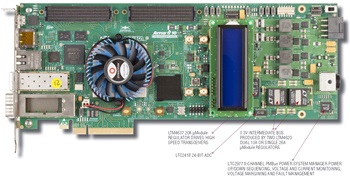
Figure 1. Arria 10 GX FPGA development kit board. All functions for power panagment and interfacing to LTpowerPlanner® (graphical softwared control) are included on the board and factory tested and verified. System debugging is minimized and performance testing (including margining) is simplified. See Table 1 for a summary of included power management components.

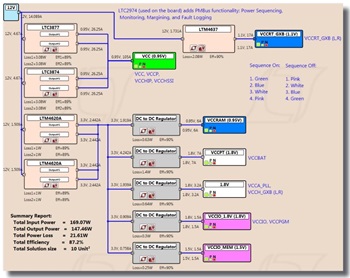
Figure 2. Power tree for Arria 10 GX FPGA board (Figure 1). Designed in LTpowerPlanner, an analytical and simple first step design tool for mapping power requirements.
Power Management for Core, System and I/O
The power management solution for high end FPGAs, including the Arria 10, should be carefully selected. A well thought out power management design can reduce PCB size, weight and complexity, as well as minimize power consumption and cooling costs. This is essential to achieve optimal system performance.
For example, the 0.95V at 105A, supplied by the 12V DC/DC regulator powering the core of the Arria 10 GX FPGA in Figure 1, has several features that complement the power saving schemes of the SoC:
- The DC/DC regulator’s integrated 6-bit parallel VID interface is used by the Arria 10’s SmartVID to control the DC/DC regulator and reduce FPGA power consumption during static and dynamic states.
- The DC/DC regulator’s very low value DCR current sensing improves efficiency by minimizing power loss in the inductor. Temperature compensation maintains the accuracy or the DCR value at higher inductor temperature.
Table 1 summarizes the Arria 10 development kit’s power rails and functions as shown in Figure 1. The table lists the parts and descriptions for each function. Visit this link and click on Arria and access technical details for the two boards presented here.
| Rail/Function | Part Number | Description |
| FPGA Core Power | LTC3877 + LTC3874 | 105A at 0.9V Regulator Seamlessly Interfaces with Arria 10 SmartVID |
| High Speed Transceivers | LTM4637 | 20A μModule Regulator |
| Power UP/DOWN Sequencing, Voltage And Current Monitoring, Voltage Margining And Fault Management | LTC2977 | 8-Channel PMBus Power System Manager |
| PowerPath™ Management | LTC4357 | High Voltage Ideal Diode Controller |
| 3.3V Intermediate Bus from 12V VIN | LTM4620 | Dual 13A or Single 26A μModule Regulator |
| Input Overvoltage Protection | LTC4365 | Overvoltage, Undervoltage and Reverse Supply Protection Controller |
| Housekeeping System Power and Power Management | LT1965, LT3082, LTC4352, LTC3025-1, LTC2418 | Low Noise Linear Regulators, 24-Bit ADC; Low Voltage Ideal Diode |
Customize the Power Tree with the LTpowerPlanner Design Tool
What if your power requirements differ from the designs exemplified in a development kit? In these cases, use the LTpowerPlanner® PC-based design tool to personalize and optimize a system’s power tree.
Start with the suggestions given in the development kit; then reorganize power blocks, alter power ratings, compute efficiency and power loss, simulate each power block, select DC/DC regulator part numbers and authenticate a customized solution.
LTpowerPlanner was used to generate the power trees (Figure 3) for the Arria 10 development kit’s FPGA and system requirements, and is available within the more encompassing LTpowerCAD® design tool, available for free download at www.analog.com/ltpowercad.

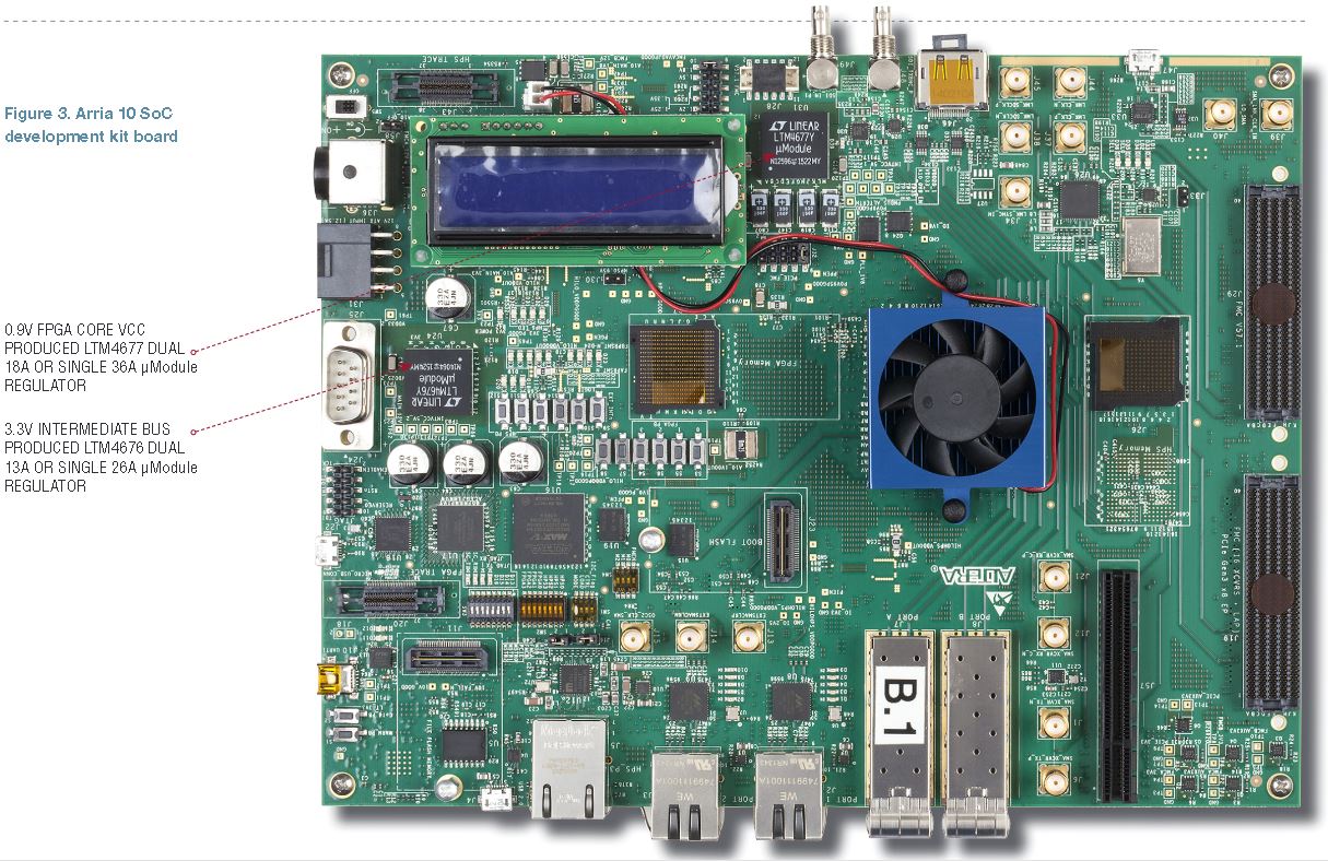
Figure 3. Arria 10 SoC development kit board

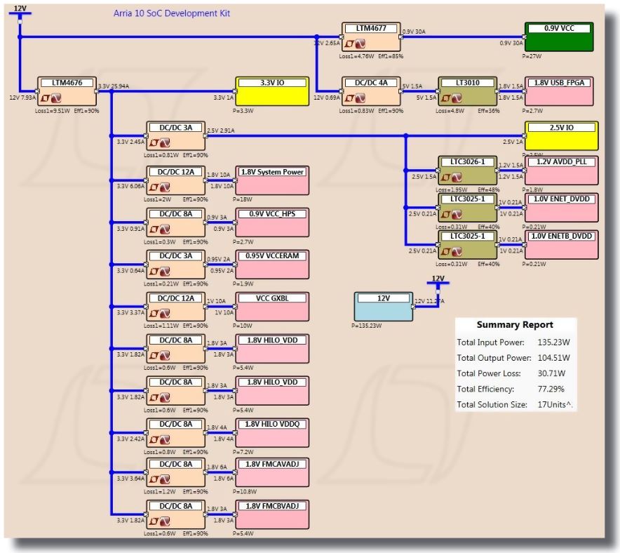
Figure 4. Power tree for Arria 10 SoC development kit board (Figure 3).
LTpowerCAD enables users to:
- Select specific Analog Devices DC/DC regulators to match a given power specification
- Select appropriate power components such as inductors, resistors and capacitors
- Optimize efficiency and power loss
- Optimize regulator loop stability, output impedance and load transient response
- Export the design to LTspice®
| Rail/Function | Part Number | General Description of Part |
| 0.9V: VCC (FPGA Core Power) | LTM4677 | Dual 18A or Single 36A μModule Regulator with Digital Power System Management |
| 3.3V: System Power | LTM4676 | Dual 13A or Single 26A μModule Regulator with Digital Power System Management |
| 1.2V: AVDD_PLL | LTC3026-1 | 1.5A Low Input Voltage VLDO™ Linear Regulator |
| 1.0V: ENET_DVDD | LTC3025-1 | 500mA Micropower VLDO Linear Regulators |
| 1.8V: USB_FPGA | LT3010 | 50mA, 3V to 80V Low Dropout Micropower Linear Regulator |
| Voltage Monitor and Control | LTC2977 | 8-Channel PMBus Power System Manager Featuring Accurate Output Voltage Measurement |
| 16-Bit ADC for Analog Input | LTC2497 | 16-Bit 8-/16-Channel Delta Sigma ADC with Easy Drive™ Input Current Cancellation and I2C Interface |
| 1.25V Voltage Reference | LT1389 | Nanopower Precision Shunt Voltage Reference |
Conclusion
Start your power management layout with confidence. Tools such as LTpowerCAD and LTpowerPlanner simplify the tasks of mapping point-of-load regulators and analyzing overall performance. The examples shown here specifically outline the benefits of using development kit design guides for Altera Arria 10 FPGAs and SoCs. These are available at www.analog.com/fpga-compatible-reference-designs. For Xilinx-based FPGA development kits, refer to www.analog.com/xilinx-fpga. Available development kits have been tested and verified by Altera, Xilinx or other developers.
Contributors
Sharad Khanal, Gerard Velcelean, Guneet Chadha and Masa Iwasaki
关于作者
关联至此文章
{{modalTitle}}
{{modalDescription}}
{{dropdownTitle}}
- {{defaultSelectedText}} {{#each projectNames}}
- {{name}} {{/each}} {{#if newProjectText}}
-
 {{newProjectText}}
{{/if}}
{{newProjectText}}
{{/if}}
{{newProjectTitle}}
{{projectNameErrorText}}
最新视频 21


