A Simple Digitally Tunable Active RC Filter
Introduction
The tuning of the cutoff frequency (fCUTOFF) of an active RC filter can be implemented using switched-capacitor circuits or continuous time circuits. In applications that require infinite tuning resolution of an any-order filter in a single IC package, a switched-capacitor approach is preferable (simply changing the clock frequency tunes fCUTOFF). In applications that require tuning a continuous time filter to just a few cutoff frequencies, tuning can be implemented using op amps, CMOS switches and resistor or capacitor arrays.
Continuous time filters can also be tuned with high resolution over a large frequency range via digital control by using DACs to multiply the RC time constant of op-amp-based integrators (for example, an 8-bit DAC-based tuner allows for 256 frequency steps). Figure 1 shows a simple, low order and low cost continuous time filter circuit. It can be tuned to a few cutoff frequencies via a Serial Peripheral Interface (SPI)1. This is a simpler alternative to using switches with resistor or capacitor arrays or multiple DACs that require a large number of active and passive components.


Figure1. An SPI tunable second order active RC filter.
Digital control through an SPI is useful in a variety of applications to control band-limiting for sensor and transducer signals. Typical applications are: accelerometers for vibration analysis, hydrophones for sonar detection, LVDTs for linear motion measurements and microphones for sound reception and recording.
An SPI-Tunable Second Order Filter
The Figure 1 circuit is a state-variable second order filter using two ICs, a low noise CMOS quad op amp (LTC6242) and a low noise dual Programable Gain Amplifier, PGA (LTC6912-X). The gains of the two LTC6912-X amplifiers (GA and GB) are independently programmed via SPI control. The SPI controlled gain settings of an LTC6912-1 are 1, 2, 5, 10, 20, 50 and 100 and for an LTC6912-2 1, 2, 4, 8, 16, 32 and 64. The Figure 1 filter has three inverting outputs providing a highpass, bandpass and lowpass frequency responses. An optional inverting amplifier connected to one of the three outputs provides for a noninverting or a differential filter output. The filter’s second order transfer function is a function of the circuit’s resonant frequency, f0 and Q values. The f0 frequency is equal to the integrator’s RC constant, the dual PGA gain and the ratio of resistors R4 and R2 (if R4 = R2 and GA = GB = Gain then f0 = Gain/2πRC). The filter’s Q value is equal the ratio of resistors R3 and R2 and the two PGA gains (if R4 = R2 and GA = GB then Q = R3/R2). The filter’s passband gain is equal to the ratio of R4/R1, R3/R1 and R2/R1 for a lowpass, bandpass and highpass filters respectively.
A Tunable Lowpass or Highpass Filter
The shape of the amplitude response of the second order depends on the f0 frequency relative to the cutoff frequency and the Q value. In a second order Butterworth highpass or lowpass response the f0 frequency is equal to fCUTOFF (f–3dB) and the filter’s Q value is equal to 0.707. In a second order Bessel highpass or lowpass response the f0 frequency is equal to 1.274 • fCUTOFF and the filter’s Q value is equal to 0.577. Figure 2 shows the tunable range of a Butterworth lowpass filter using an 100Hz integrator frequency (R = 1.58MΩ, ±1% and C = 1000pF, ±5%) and an LTC6912-2 to tuned the filter’s fCUTOFF from 100Hz to 6.4kHz. Figure 3 shows the tunable range of a Butterworth highpass filter that is the mirror oposite of the lowpass filter reponse of Figure 2. The output response to a step change is approximately equal to 5/fCUTOFF, (if the step change is to a 1kHz fCUTOFF then the filter settles five milli-seconds after a step change). The maximum tunable f0 frequency is a function of the gain-bandwidth product of the op amps and the circuit’s sensitivity to the highest PGA gain that is used for tuning. For the amplifiers shown, based on empirical data, a maximum f0 of 800kHz/[Q • Gain] limits gain error to ≤2dB). For example, if only the lowest 1, 2, 5 and 10 gains of an LTC6912-1 are used for tuning, a second order Butterworth lowpass filter (f0 = fCUTOFF) can be tuned to 110kHz (maximum f0 = 800kHz/[0.707 • 10]).

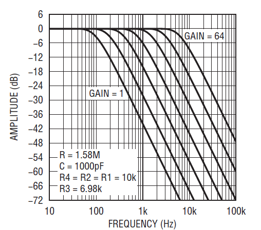
Figure 2. Tunable second order Butterworth lowpass response using the LTC6912-2.

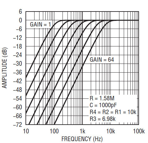
Figure 3. Tunable second order Butterworth highpass response using the LTC6912-2.
A Tunable Bandpass Filter
The –3dB bandwidth of a second order filter is equal to the center frequency (fCENTER) divided by the Q value (bandwidth = fCENTER/Q). The sensitivity of the second order bandpass filter to the tolerance of the integrator’s RC values is proportional to the filter’s Q. Typically with a Q ≤ 4, using a ±1% R and a ±5% C for the filter’s two integrators is practical for a second bandpass filter. The sensentivity of the second order bandpass filter with Q > 4 increases rapidly for each unit of Q increase and the filter’s two integrators should use ±1% RC components.
Figure 4 shows the bandpass filter of Figure 1 tuned from 2kHz to 16kHz using a 2kHz integrator frequency (R = 205k, ±1% and C = 390pF, ±5%) and an LTC6912-2 with gain settings 1, 2, 4, and 8. The tuned center frequencies responses of Figure 4 are 2.73% lower than the design values of 2kHz, 4kHz, 8kHz and 16kHz and equal to the error of the circuit’s RC values of the two integrators (measured values of approximately 206k for each R and 403pF for each C). The gain error at 16kHz is due to the filter’s f0 frequency approaching the maximum f0 for a Q = 4 and a PGA gain equal to 8 (maximum f0 = 25kHz = 800kHz/{4 • 8]). The maximum f0 frequency is a function of the gain-bandwidth product of the LTC6912-X op amps.

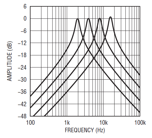
Figure 4. Tunable second order bandpass filter using an LTC6912-1 with gains 1–8.
Other Filter Options
Figure 5 shows an example of a second order notch filter. The notch filter’s integrator frequency is 500Hz (1/[2π • 316kΩ • 1000pF]) and with PGA gains 1, 2, 4 and 8 the notch frequency is tuned to 500Hz, 1kHz, 2kHz and 4kHz respectively. Any of the filters discussed above can be made into SPI-tunable fourth order filters by cascading two second order circuits.

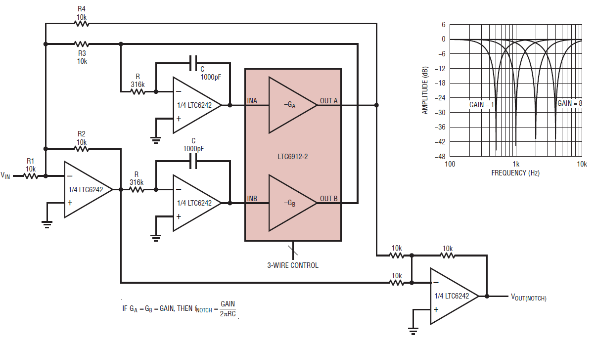
Figure 5. An SPI-tunable second order notch filter.
关于作者
最新视频 21


