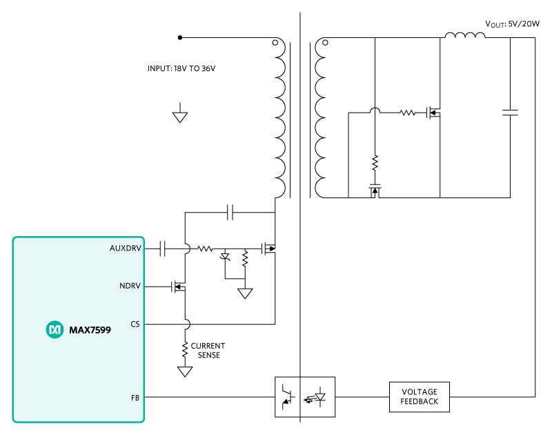
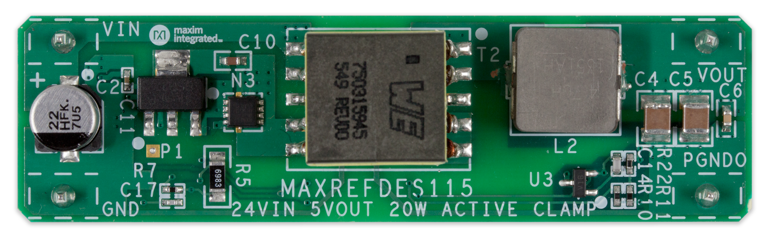
The MAX17599 low IQ active-clamp current-mode PWM controller contains all the control circuitry required for designing wide-input isolated forward-converter industrial power supplies.
The device includes an AUX driver that drives an auxiliary MOSFET (clamp switch) that helps implement the active-clamp transformer reset topology for forward converters. This reset topology has several advantages, including reduced voltage stress on the switches, transformer size reduction due to larger allowable flux swing, and improved efficiency due to elimination of dissipative snubber circuitry. Programmable dead time between the AUX and main driver allows for zero voltage switching.
Primary Power Stage
The active-clamp transformer primary side is driven by an n-channel MOSFET (N1) and a p-channel MOSFET (P1). While N1 is on, power is delivered to the secondary, and magnetizing energy is being stored in the transformer. During this time, P1 is off, and the clamp capacitor (C12) is charged at a constant voltage level.
When N1 turns off, the leakage and magnetizing currents charge up the drain-to-source capacitance of N1. Once the drain-to-source voltage of N1 exceeds the voltage across the clamp capacitor, the body diode of P1 begins to conduct. With the body diode of P1 conducting, the magnetizing current begins to charge the clamp capacitor.
After the body diode of P1 conducts, P1 turns on. This provides zero current switching for P1. The clamp capacitor continues to charge until the magnetizing current is reduced to 0A. At this point, the magnetizing current reverses, and the clamp capacitor begins to discharge until the P1 turns off.
After P1 turns off, the clamp capacitor remains at a fixed voltage. There is a fixed delay before N1 turns on. During this delay, the energy in the parasitic components discharges the VDS of N1 towards VIN. This allows softer turn on and lower switching losses for N1.
The MAX17599 NDRV pin drives N1 while the AUXDRV pin is level shifted through C11, R14, and D4, and then drives P1.
Secondary Power Stage
The secondary power stage consists of the synchronous rectifiers (N1, N2), and the output filters (L2, C4, C5, C6).
When the primary n-FET (N3) is turned ON, the input power is transferred instantaneously to the output through forward conducting MOSFET N2. During the turn-off period, the output inductor current freewheels through MOSFET N1.
The voltage on the input end of the filter inductor is a typical buck converter square wave. The inductor and output capacitors filter the square wave to produce a DC voltage on the output.
Feedback Control Loop
The feedback network is constructed using a TLV431B programmable shunt regulator, a 3000V isolation optocoupler, and other RC components.
Startup Voltage and Input Overvoltage Protection Setting (EN/UVLO, OVI)
The EN/UVLO pin in the MAX17599 serves as an enable/disable input, as well as an accurate programmable under voltage lockout (UVLO) pin. The MAX17599 does not begin startup operations unless the EN/UVLO pin voltage exceeds 1.21V (typ). The MAX17599 turns off if the EN/UVLO pin voltage falls below 1.15V (typ). A resistor divider from the input DC bus to ground can be used to divide down and apply a fraction of the input DC voltage to the EN/UVLO pin. The values of the resistor divider can be selected so that the EN/UVLO pin voltage exceeds the 1.21V (typ) turn on threshold at the desired input DC bus voltage. The same resistor divider can be modified with an additional resistor, ROVI, to implement overvoltage input protection in addition to the EN/UVLO functionality. When the voltage at the OVI pin exceeds 1.21V (typ), the MAX17599 stops switching. Switching resumes with soft-start operation, only if the voltage at the OVI pin falls below 1.15V (typ).