Linear Regulator Converts 3.3V to 2.9V at 2A
Abstract
An op amp and p-channel MOSFET make a low dropout high current linear regulator that features excellent transient response to load steps. Dropout is 300mV at a 2A load.
Linear regulators (vs. switching types) are often the best choice for generating supply voltages below 3.3V. At low output voltage and moderate load currents, the linear type is less expensive and requires less space, yet maintains reasonable efficiency. The circuits of Figure 1, for example, have efficiencies higher than 87%.
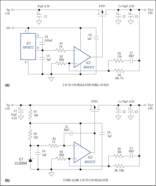
Figure 1. These linear regulators generate 2A at 2.9V, either with the help of a 5V bus (a) or from 3.3V alone (b).
Dropout voltage for the available "low-dropout" linear regulators may not be low enough for the load current desired. The Figure 1 circuits, therefore, employ low-threshold p-channel MOSFETs that drop only 300mV at 2A. If available, a 5V bus should power the op amp and the 2.5V reference (Figure 1a). The higher rail voltage improves transient response by enabling the op amp to drive the MOSFET faster. (Power-management circuitry in the newer processors can change load current within tens of nanoseconds.)
The 10MHz op amp allows common-mode inputs from ground to within 1.9V of the positive rail, so 3.3V operation allows insufficient room for a 2.5V reference. With a 1.2V reference (Figure 1b) the 3.3V circuit provides ±3% initial output accuracy and ±5% regulation (for the fixture tested) over the allowed extremes for line, load, temperature, and supply-voltage transients. The Figure 1a circuit measured ±4% for the extremes and ±2% for initial accuracy. Both circuit outputs change less than 1mV for a 5% VIN change, and only 3mV for a 0A to 2A load change (see Figure 2 for the effect of a 1A to 2A load change).
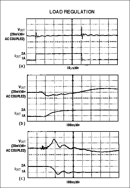
Figure 2. A step change in load current (a) for the figure 1 curcuits is streched from 10µs to 100ns per division for the 1A to 2A case (b) and the 2A to 1A case (c). Vertical resolution is 20mV/div for the output voltage (top traces) and 1A/div for the load current (bottom traces).
Layout is critical if the circuits are to accommodate transient rise times faster than 100ns. The regulator should be close to the load, and VOUT should be sensed at the load. The op amp and reference should have a single-point ground to prevent ground bounce and noise from upsetting the feedback loop.
Because the initial edge of any transient will be absorbed by the 10µF output capacitors, these components (such as the Sanyo OS-CON types shown) must have very low ESR. To minimize the effect of lead inductance in surface-mount capacitors, you can reduce the lead lengths virtually to zero by routing output current right through the capacitors' metallized contacts.
A related idea appeared in the 3/16/95 issue of EDN.