Bridge from USB to I²C
Abstract
This circuit provides a direct I2C interface to your PC's USB port. A USB to 1-Wire® dongle supplies the PC with a 1-Wire master, which controls a 1-Wire I/O extender. This I/O extender has two bidirectional open drain ports, which the PC can write to and read from. By generating the right logic signals on these two ports, the PC can emulate an I2C master.
Introduction
A similar version of this article appeared in Dutch in the February 2009 issue and in German, French, and English in the March 2009 issue of Elektor magazine.
The LabVIEW® software discussed in this application note is available for download.
When you need a direct I2C interface to your PC, several options are available. The PC's parallel port, for instance, can emulate an I2C master (see application note 3230, "How to use a PC's parallel port to communicate with 2-wire devices"). New PCs, however, often lack this port, and modern variants of Windows® (Windows XP® and Windows Vista®) do not allow easy access to it.
A better approach is to use the USB port, but that technique requires a complex driver and often a microcontroller as well, which in turn requires firmware. Not something you can build in an afternoon! Numerous commercial versions are available, but they aren't cheap. The circuit of Figure 1, on the other hand, can be built quickly, and it operates with a variety of programming languages such as LabVIEW and Visual Basic.
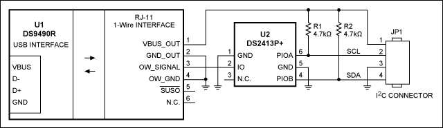
Figure 1. This circuit provides an I2C interface to a computer's USB port.
U1 (DS9490R) is a USB-to-1-Wire bridge and adds a 1-Wire master to the PC. A 1-Wire I/O extender (U2, DS2413P) connected to the 1-Wire net offers two bidirectional open-drain ports, controllable by the PC via U1. That is all the hardware needed to create an I2C master.
Software
For microcontrollers that lack a hardware I2C master, "bit banging" is a proven method for implementing a software I2C master. That is the technique used to enable a software I2C master for this platform.
Software generates the I2C signals by controlling the logic levels of U2's PIOA and PIOB (pins 6 and 4). To create the start condition, for instance, SDA must transition from high to low while SCL is high. Drive SCL (PIOA) high, then SDA (PIOB) high, and then pull SDA low. Thus, software implements the I2C master by controlling PIOA and PIOB. A flow chart from the DS2413 data sheet shows this PIO function (Figure 2).
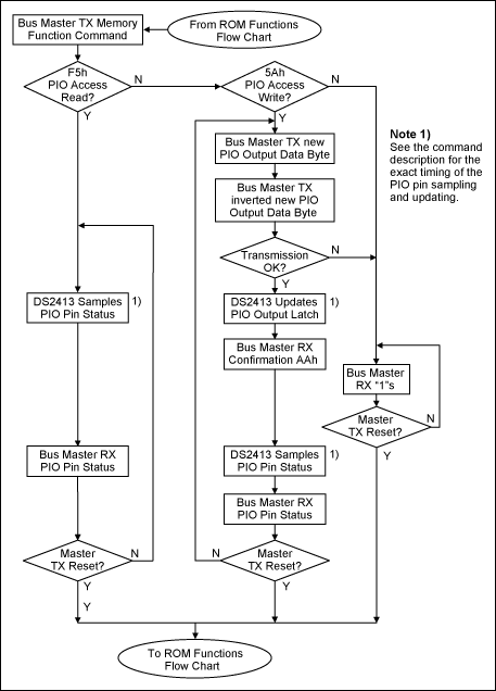
Figure 2. Flow chart for the PIO function, taken from the DS2413 data sheet.
To change the PIO outputs, you must first address the part via ROM functions. This system includes only a single 1-Wire slave, so you can skip the complex addressing procedure using the "skip ROM" command. You then write to the PIO output latches by sending a "5A" command. The 1-Wire I/O extender (U2) includes an 8-bit register whose two LSBs connect to PIOA and PIOB. (The other six bits are don't cares.)
To change the logic state, new data is sent twice: once as is, and once inverted. The slave (U2) confirms error-free reception by returning an "AA" command to the master, and concludes by sending the new output state as well. The whole sequence can now start over, or be aborted by a reset from the 1-Wire master. Thus, you must transfer four bytes (not counting the Skip ROM and 5A commands) for each output change. For example, you must execute the following sequence to generate the I2C start command:
| Master Mode | Data | Comments |
| TX | (Reset) | Reset the bus |
| RX | (Presence) | DS2413 is present |
| TX | 0xCC | Skip ROM |
| TX | 0x5A | Write PIO register |
| TX | 0xFF | SCL=1 & SDA=1 |
| TX | 0x00 | Inverted data |
| RX | 0xAA | Data is received |
| RX | 0x0F | Return output state |
| TX | 0xFD | SCL=1 & SDA=0 |
| TX | 0x02 | Inverted data |
| RX | 0xAA | Data received |
| RX | 0x2D | Return output state |
Similar sequences implement other events such as send byte, acknowledge, and stop.
Maxim offers a software driver for the DS9490, and also a 1-Wire Software Development Kit (SDK) for Windows that supports the Microsoft .NET platform. To illustrate, we can implement an I2C master in LabVIEW, using its .NET support. That works only if the 1-Wire driver is installed with .NET support. Another prerequisite is to install the Microsoft .NET framework and Visual J# redistributable package. For details, see application note 155, "1-Wire® software resource guide device description."
To prevent other applications from accessing the 1-Wire net, the VI "I2C Initialize" (where VI is a LabVIEW term meaning virtual instrument), initializes U1 and gives LabVIEW exclusive access to the 1-Wire net (Figure 3). You then issue a 1-Wire reset followed by a skip command (CC), and conclude with a PIO write command (5A).
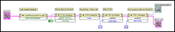
Figure 3. The VI "I2C Initialize" initializes the DS2413, after which it is ready to receive I/O data.
The slave (U2) is now ready to accept data for the PIOs. The VI "I2C clock" toggles the SCL line from low to high (Figure 4). SDA can be set high or low, and the VI returns the SDA state. You can write a complete byte by calling this function 8 times in a row (one for each bit transmitted). If the slave is returning data, SDA is driven high by the master. To transmit "0" the slave can pull SDA low (this is OK, because PIOB is an open-drain output). Because U2 automatically returns the updated output state, no special read action is required (see the VIs "Send I2C byte" and "Get I2C byte").
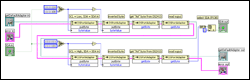
Figure 4. The VI "I2C clock" toggles SCL from low to high. SDA can be set or reset for "I2C write" actions and read for "I2C read" actions.
The VIs "I2C start," "I2C stop," and "I2C acknowledge" use the same structure to generate appropriate SDA and SCL signals. By combining these VIs, you can program a complete I2C read or write session. To illustrate a communication session (Figure 5), we read Register 0 of a Real-Time Clock (DS1337). That device then answers with 0x39, which is the content of the register that counts the seconds. The register address is set to 0x00, the slave address to 0xD0, and the number of bytes to be read is set to 1. A scope image (Figure 6) shows the signals generated by the circuit for these settings.
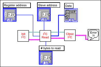
Figure 5. Example of how to read a register, using the Figure 1 circuit.
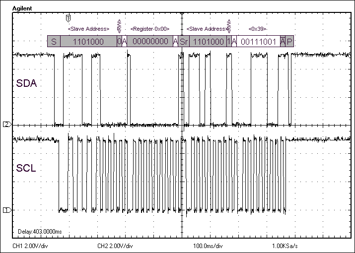
Figure 6. Read register 0 of DS1337. S=start, A=acknowledge, Sr=repeated start, and P=Stop. From master to slave is shaded; from slave to master is white.
Because the software overhead is large, the rate at which this circuit generates signals is limited to approximately 20bps. The idea can be implemented in different programming languages, however. The Maxim website offers several 1-Wire example programs you can use as a starting point.