Design Note 224
Design Note 224: Active Voltage Positioning Reduces Output Capacitors
Introduction
Power supply performance, especially transient response, is key to meeting today’s demands for low voltage, high current microprocessor power. In an effort to minimize the voltage deviation during a load step, a technique that has recently been named “active voltage positioning” is generating substantial interest and gaining popularity in the portable computer market. The benefits include lower peak-to-peak output voltage deviation for a given load step, without having to increase the output filter capacitance. Alternatively, the output filter capacitance can be reduced while maintaining the same peak-to-peak transient response.
Basic Principle
The term “active voltage positioning” (AVP) refers to setting the power supply output voltage at a point that is dependent on the load current. At minimum load, the output voltage is set to a slightly higher than nominal level. At full load, the output voltage is set to a slightly lower than nominal level. Effectively, the DC load regulation is degraded, but the load transient voltage deviation will be significantly improved. This is not a new idea, and it has been observed and described in many articles. What is new is the application of this principle to solve the problem of transient response for microprocessor power. Let’s look at some numbers to see how this works.

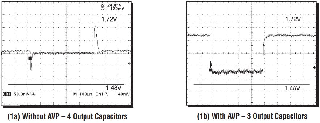
Figure 1. Transient Response with Load Step from 0A to 12A.
Assume a nominal 1.5V output capable of delivering 15A to the load, with a ±6% (±90mV) transient window. For the first case, consider a classic converter with perfect DC regulation. Use a 10A load step with a slew rate of 100A/μs. The initial voltage spike will be determined solely by the output capacitor’s equivalent series resistance (ESR) and inductance (ESL). A bank of eight 470μF, 30mΩ, 3nH tantalum capacitors will have an ESR = 3.75mΩ and ESL = 375pH. The initial voltage droop will be (3.75mΩ • 10A) + (375pH • 100A/μs) = 75mV. This leaves a 1% margin for set point accuracy. The voltage excursion will be seen in both directions, for the full load to minimum load transient and for the minimum load to full load transient. The resulting deviation is 2 • 75mV = 150mV peak-to-peak (Figure 2a).

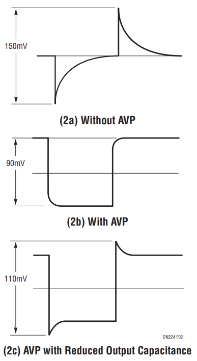
Figure 2. Transient Response Comparison.
Now look at the same transient using active voltage positioning. At the minimum load, purposefully set the output 3% (45mV) high. At full load, the output voltage will be set 3% low. During the minimum load to full load transient, the output voltage starts 45mV high, drops 75mV initially, and then settles to 45mV below nominal. For the full load to minimum load transient, the output voltage starts 45mV low, rises 75mV to 35mV above nominal, and settles to 45mV above nominal. The resulting deviation is now only 2 • 45mV = 90mV peak-to-peak (Figure 2b). Now reduce the number of output capacitors from eight to six. The ESR = 5mΩ and ESL = 500pH. The transient voltage step is now (5mΩ • 10A) + (500pH • 100A/μs) = 100mV. With the 45mV offset, the resultant change is ±55mV around center, or 110mV peak-to-peak (Figure 2c). The initial specification has been easily met with a 25% reduction in output capacitors.
An added benefit of voltage positioning is an incremental reduction in CPU power dissipation. With the output voltage set to 1.50V at 15A, the load power is 22.5W. By decreasing the output voltage to 1.47V, the load current is 14.7A and the load power is now 21.6W. The net saving is 0.9W.
Basic Implementation
In order to implement voltage positioning, a method for sensing the load current is required. This information must then be used to move the output voltage in the correct direction. For a current mode controller, such as the LTC1736, a current sense resistor is already used. By controlling the error amplifier gain, we can achieve the desired result.
Current Mode Control Example – LTC®1736
Figure 3 shows the basic power stage and feedback compensation circuit for the LTC1736. In a non-AVP implementation, RA1 and RA2 are removed and CC and RC installed. The corresponding transient response with 20V input and 1.6V output is shown in Figure 1a. In order to implement voltage positioning, we will control the error amplifier gain at the ITH pin. The internal gm amplifier gain is equal to gm • RO, where gm is the transconductance in mmhos, and RO is the output impedance in kohms. The voltage at the ITH pin is proportional to the load current, where 0.48V = min load, 1.2V = half load, and 2V = full load in this application. RO = 600kΩ and gm = 1.3mmho. By setting a voltage divider to 1.2V from the 5V INTVCC, the gain can be limited without effecting the nominal DC set point at half load. The Thevenin equivalent resistance is seen to be in parallel with the amplifiers RO. Using the values shown in Figure 3 for RA1 and RA2, the effective RO will be 600k||91k||27k = 20.12kΩ. The voltage deviation at the amplifier input ΔVFB = ΔVITH/(gm • ROeff). ΔVFB = (2.0V-0.48V)/(1.3mmho • 20.12kΩ) = 58mV, which is ±29mV from the nominal half load set point.

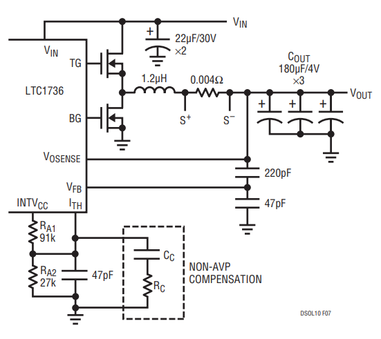
Figure 3. LTC1736 with AVP.
Care should be taken to keep the amplifier input from being pulled more than ±30mV from its nominal value, or non-linear behavior may result. The DC reference voltage at VFB is 0.8V and Vout is set for 1.6V, so ΔVOUT = 2 • ΔVFB = 116mV. The resulting transient response is shown in Figure 1b. The transient performance has been improved, while using fewer output capacitors.
The optimal amount of AVP offset is equal to ΔI • ESR. Figure 1b exhibits this condition.
作者
