AN-937: Designing Amplifier Circuits: How to Avoid Common Problems
Introduction
When compared to assemblies of discrete semiconductors, modern operational amplifiers (op-amps) and instrumentation amplifiers (in-amps) provide great benefits to designers. Although there are many published articles on circuit applications, all too often, in the haste to assemble a circuit, basic issues are overlooked leading to a circuit that does not function as expected. This application note discusses the most common design problems and offers practical solutions.
Missing DC Bias Current Return Path
One of the most common application problems encountered is the failure to provide a dc return path for bias current in accoupled op-amp or in-amp circuits. In Figure 1 a capacitor is connected in series with the noninverting (+) input of an op-amp. This ac coupling is an easy way to block dc voltages associated with the input voltage (VIN). This is especially useful in high gain applications, where even a small dc voltage at amplifier input can limit the dynamic range or even result in output saturation. However, capacitive coupling into a highimpedance input without providing a dc path for current flowing in the positive input leads to problems.

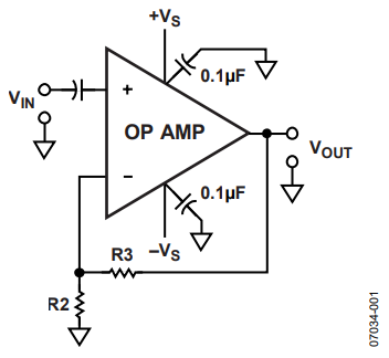
Figure 1. A nonfunctional AC-coupled op-amp circuit.
The input bias current flows through the coupling capacitor, charging it, until the common-mode voltage rating of the amplifier’s input circuit is exceeded or the output is driven into limits. Depending on the polarity of the input bias current, the capacitor charges up toward the positive supply voltage or down toward the negative supply. The bias voltage is amplified by the closed-loop dc gain of the amplifier.
This process can be lengthy. For example, an amplifier with a field effect transistor (FET) input, having a 1 pA bias current, coupled via a 0.1-µF capacitor, has an IC charging rate, I/C, of:
10-12/10-7 = 10 µV per sec
or 600 µV per minute. If the gain is 100, the output drifts at 0.06 V per minute. Therefore, a casual lab test, using an accoupled scope, may not detect this problem, and the circuit may not fail until hours later. It is important to avoid this problem altogether.
Figure 2 shows a simple solution to this common problem. In this example, a resistor is connected between the op-amp input and ground to provide a path for the input bias current. To minimize offset voltages caused by input bias currents, which track one another when using bipolar op-amps, R1 is usually set equal to the parallel combination of R2 and R3.

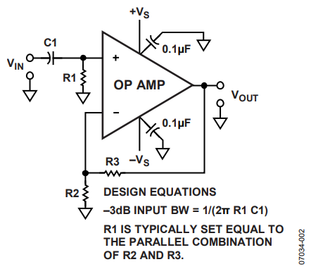
Figure 2. Correct method for AC-coupling an op-amp input for dual-supply operation.
Note, however, that this resistor always introduces some noise into the circuit, so there is a trade-off between circuit input impedance, the size of the input coupling capacitor needed, and the Johnson noise added by the resistor. Typical resistor values are generally in the range of about 100,000 Ω to 1 MΩ.
A similar problem can affect an in-amp circuit. Figure 3 shows in-amp circuits that are ac-coupled using two capacitors, without providing an input bias current return path. This problem is common with in-amp circuits using both dual-power supplies (Figure 3a) and single-power supplies (Figure 3b).

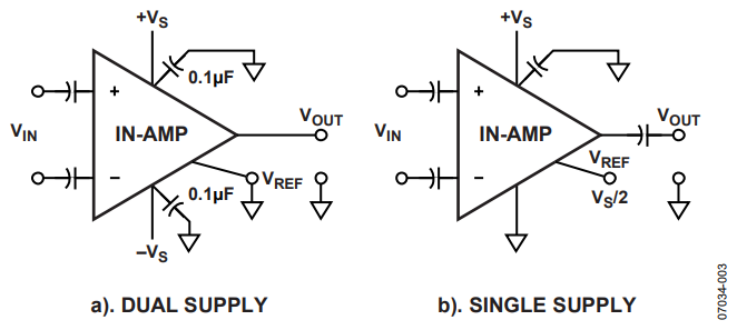
Figure 3. Nonfunctional AC-coupled in-amp circuits.
The problem can also occur with transformer coupling, as in Figure 4, if no dc return path to ground is provided in the transformer’s secondary circuit.

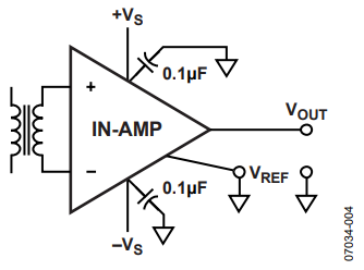
Figure 4. A nonfunctional transformer-coupled in-amp circuit.
Simple solutions for these circuits are shown in Figure 5 and Figure 6. A high value resistance (RA, RB) is added between each input and ground. This is a simple and practical solution for dual-supply in-amp circuits. The resistors provide a discharge path for input bias currents. In the dual-supply example, both inputs are referenced to ground. In the single-supply example, the inputs can be referenced either to ground (VCM tied to ground) or to a bias voltage, usually one-half the maximum input voltage range.

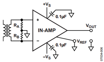
Figure 5. Correct method for transformer input coupling to an in-amp.

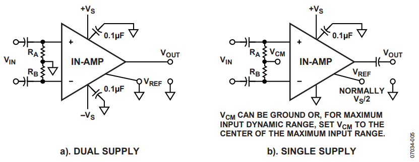
Figure 6. A high value resistor between each input and ground supplies the necessary bias current return path.
The same principle can be used for transformer-coupled inputs (Figure 5) unless the transformer secondary winding has a center tap, which can be grounded or connected to VCM. In these circuits, there is a small offset voltage error due to mismatches between the resistors and/or the input bias currents. To minimize these errors, a third resistor, about 1/10th their value (but still large compared to the differential source resistance), can be connected between the two in-amp inputs (thus bridging both resistors).
Supplying Reference Voltages for In-Amps, Op-Amps, and ADCs
Figure 7 shows a single-supply circuit where an in-amp is driving a single-ended analog-to-digital converter (ADC). The amplifier reference provides a bias voltage corresponding to zero differential input, and the ADC reference provides the scale factor. A simple RC low-pass antialiasing filter is often used between in-amp output and ADC input to reduce out-of-band noise. Often designers are tempted to use simple approaches, such as resistance dividers, to supply the in-amp and ADC reference voltages. This can lead to errors with some in-amps.

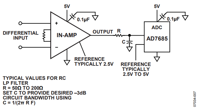
Figure 7. An in-amp drives an ADC in a typical single-supply circuit.
Correctly Providing In-Amp Reference Voltage
A common assumption is that the in-amp reference-input terminal is at high impedance, since it is an input. Therefore, a designer may be tempted to connect a high impedance source, such as a resistive divider, to the reference pin of an in-amp. This can introduce serious errors with some types of instrumentation amplifiers (see Figure 8).

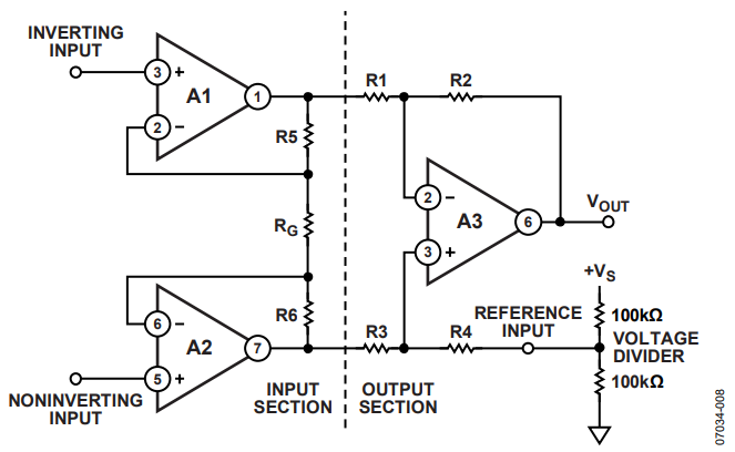
Figure 8. Incorrect use of a simple voltage divider to directly drive the reference pin of a 3 op-amp instrumentation amplifier.
For example, a popular in-amp design configuration uses three op-amps connected as shown in Figure 8. The overall signal gain is:
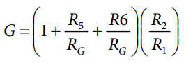
where:
The gain for the reference input (if driven from low impedance) is unity. However, in this example, the in-amp has its reference pin tied directly to a simple voltage divider. This unbalances the symmetry of the subtractor circuit and the division ratio of the voltage divider. This reduces the in-amp’s common-mode rejection and its gain accuracy. However, in some cases, R4 is accessible, thus its resistance value can be reduced by an amount equal to the resistance looking back into the paralleled legs of the voltage divider (50 kΩ in this case). In this case, the circuit behaves as though a low impedance voltage source equal to one-half the supply voltage is applied to the original value of R4. In addition, the subtractor accuracy is maintained.
This approach can not be used if the in-amp is provided as a closed single package (an IC). Another consideration is that the temperature coefficients of the resistors in the voltage divider should track those of R4 and the other resistors in the subtractor. Finally, the approach locks out the possibility of having the reference be adjustable. If, on the other hand, one attempts to use small resistor values in the voltage divider to make the added resistance negligible, this increases power supply current consumption and increases the dissipation of the circuit. Such brute force is not a good design approach.
Figure 9 shows a better solution, using a low power op-amp buffer between the voltage divider and the in-amp reference input. This eliminates the impedance matching and temperature tracking problem and allows the reference to be easily adjustable.


Figure 9. Driving the reference pin of an in-amp from the low impedance output of an op-amp.
Preserving PSR When Amplifiers are Referenced from the Supply Rail Using Voltage Dividers
An often-overlooked consideration is that any noise, transients, or drift of power supply voltage, VS, fed in through the reference input adds directly to the output, attenuated only by the divider ratio. Practical solutions include bypassing and filtering, and even generating the reference voltage with a precision reference IC, such as the ADR121, instead of tapping off VS.
This consideration is important when designing circuits with both in-amps and op-amps. Power supply rejection (PSR) techniques isolate an amplifier from power supply hum, noise, and any transient voltage variations present on the power rails. This is important because many real world circuits contain, connect to, or exist in environments that offer less than ideal supply voltage. In addition, ac signals present on the supply lines can be fed back into the circuit, amplified, and, under the right conditions, stimulate a parasitic oscillation.
Modern op-amps and in-amps provide substantial low frequency power supply rejection as part of their design. This is something that most engineers take for granted. Many modern op-amps and in-amps have PSR specs of 80 dB to over 100 dB, reducing the effects of power supply variations by a factor of 10,000 to 100,000. Even a modest PSR specification of 40 dB isolates supply variations from the amplifier by a factor of 100. Nevertheless, high frequency bypass capacitors (such as those in Figure 1 through Figure 7) are always desirable and often essential. In addition, when designers use a simple resistance divider on the supply rail and an op-amp buffer to supply a reference voltage for an in-amp, any variations in power supply voltage are passed through this circuitry with little attenuation and add directly to the in-amp output level. Therefore, unless low-pass filtering is provided, the normally excellent PSR of the IC is lost.
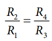
In Figure 10, a large capacitor is added to the voltage divider to filter its output from power supply variations and preserve PSR. The −3 dB pole of this filter is set by the parallel combination of R1/R2 and Capacitor C1. The pole should be set approximately 10 times lower than the lowest frequency of concern.

Figure 10. Decoupling the reference circuit to preserve PSR.
The cookbook values shown in Figure 10 provide a −3 dB pole frequency of approximately 0.03 Hz. The small (0.01 µF) capacitor across R3 minimizes resistor noise.
The filter takes time to charge up. Using the cookbook values, the rise time at the reference input is several time constants (where T = R3Cf = 5 s), or about 10 to 15 seconds.
The circuit in Figure 11 offers a further refinement. In this case, the op-amp buffer operates as an active filter, which allows the use of much smaller capacitors for the same amount of power supply decoupling. In addition, the active filter can be designed to provide a higher Q and thus give a quicker turn-on time.

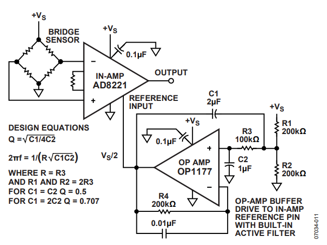
Figure 11. An op-amp buffer connected as an active filter drives the reference pin of an in-amp.
This circuit was tested with the component values shown in Figure 11, with 12 V applied, and a 6 V filtered reference voltage provided to the in-amp. A 1 V p-p sine wave of varying frequency was used to modulate the 12 V supply, with the in-amp gain set to unity. Under these conditions, as frequency was decreased, no ac signal was visible on an oscilloscope, at VREF, or at the in-amp output, until approximately 8 Hz. Measured supply range for this circuit ranged from 4 V to greater than 25 V, with a low level input signal applied to the in-amp. Circuit turn-on time was approximately two seconds.
Decoupling Single-Supply Op-Amp Circuits
Single-supply op-amp circuits require biasing of the input common-mode level to handle the positive and negative swings of ac signals. When this bias is provided from the power supply rail using voltage dividers, adequate decoupling is required to preserve PSR.
A common, though incorrect, practice is to use a 100 kΩ/100 kΩ resistor divider with a 0.1 µF bypass capacitor to supply VS/2 to the noninverting pin of the op-amp. Using these values, power supply decoupling is often inadequate because the pole frequency is only 32 Hz.
Circuit instability (motor boating) Figure 12 (noninverting) and Figure 13 (inverting) show circuits to accomplish VS/2 decoupled biasing for best results. In both cases, bias is provided at the noninverting input, feedback causes the inverting input to assume the same bias, and unity dc gain biases the output to the same voltage. Coupling Capacitor C1 rolls the low frequency gain down toward unity from BW3.

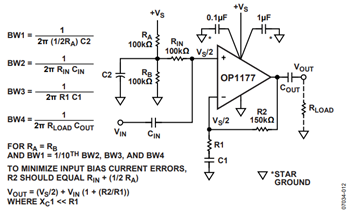
Figure 12. A single-supply noninverting amplifier circuit showing correct power suppy decoupling. Midband gain = 1 + R2/R1.

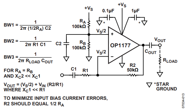
Figure 13. Proper decoupling for a single-supply inverting amplifier circuit. Midband gain = –R2/R1.
A good rule of thumb when using a 100 kΩ/100 kΩ voltage divider, as shown in Figure 12, is to use a C2 value of at least 10 µF for a 0.3 Hz −3 dB roll-off. A value of 100 µF (0.03 Hz pole) should be sufficient for practically all circuits.
作者
