AN-2562: 5V Regulator Supplies High Transient Current for Dynamic Power Controlled DAC
Circuit Function and Benefits
The circuit shown in Figure 1 provides a unique power saving solution for a digital-to-analog converter (DAC)-based, 4 mA to 20 mA output circuit. To provide sufficient headroom for typical resistive loads between 10 Ω and 1000 Ω, traditional 4 mA to 20 mA output driver stages must operate on at least 20 V (plus some additional headroom) to provide a sufficient voltage to drive high value resistive loads. For low value resistive loads, however, the fixed value, high voltage supply results in significant internal power dissipation that can affect DAC accuracy and require additional heat sinking.
The AD5755 quad 16-bit DAC has four independent high efficiency, internal dc-to-dc converters that drive the four output stages at a dynamically adjusted boost voltage based on sensing the actual output voltage of the 4 mA to 20 mA driver. The boost circuit maintains several volts of headroom on the output stage, regardless of the load resistance, thereby reducing the maximum internal power dissipation by a factor of approximately 4× for a 24 mA output current into a 10 Ω load.
The internal dc-to-dc converters require an external 5 V supply and can draw significant currents when the DAC outputs full-scale slew. A high efficiency external dc-to-dc converter circuit based on the ADP2300 is driven from the 15 V and supplies this voltage. The ADP2300 has excellent transient response to large current steps up to 800 mA and ensures proper operation of the boost converters as well as eliminating the need for a separate 5 V supply.
The entire circuit operates on ±15 V supplies that allow the DAC to provide voltage outputs that cover the industrial signal level range of up to ±10 V in addition to the 4 mA to 20 mA outputs. This combination of parts is a low cost, power efficient solution that minimizes the number of external components required and that ensures 16-bit performance for varying load conditions.


Circuit Description
This circuit enhances the slew rate control and dynamic power control features of the AD5755 to create a more complete and robust DAC solution. By implementing a simple step-down dc-to-dc converter using the ADP2300, the circuit can provide higher than normal supply currents that are required when slewing the AD5755 outputs.
The AD5755 behaves like any standard DAC converting digital data to analog current (for example, 0 mA to 20 mA, 4 mA to 24 mA, or 0 mA to 24 mA) or voltage outputs (0 V to 5 V, 0 V to 10 V, ±5 V, or ±10 V). The AD5755 operates with an extended AVSS power supply range to −26.4 V, and an AVDD range to +33.0 V.
Power Dissipation Control
In standard, current controlled module or actuator designs, the load resistor value can range from typically 50 Ω to 750 Ω, but it can be as low as 10 Ω or as high as 1 kΩ. The 4 mA to 20 mA output driver stage must operate on a supply voltage that provides sufficient headroom for the full range of the load resistor values. For example, when driving 24 mA into a 1 kΩ load, a supply voltage of greater than 27 V is required, assuming a 3 V headroom is needed. In this case, the internal package power dissipation due to the output driver is 3 V × 24 mA = 72 mW. However, when driving a 10 Ω load with the same 27 V supply voltage, the internal power dissipation of the driver is approximately 27 V × 24 mA = 648 mW. For a quad DAC, this is greater than 2.5 W.
The AD5755 circuitry senses the output voltage and dynamically regulates the boost supply voltage to meet supply voltage requirements plus a sufficient amount of headroom. For 24 mA output into 10 Ω, the boost voltage of 7.4 V results in an internal power dissipation of only 7.4 V × 24 mA = 178 mW. This represents nearly a 4× reduction in power vs. the unregulated case.
A separate boost supply voltage is generated for each of the four DAC outputs by four independent dc-to-dc converters operating on a 5 V input.
DC-to-DC Converters
The AD5755 contains four independent, on-board dc-to-dc converters. They provide dynamic control of the VBOOST_X supply voltage for each individual channel. Figure 2 shows the discrete components needed for the dc-to-dc circuitry, and the following sections describe the operation of this circuitry.


It is recommended to place a 10 Ω, 100 nF low-pass RC filter after CDCDC. This consumes a small amount of power; however, it reduces the amount of ripple on the VBOOST_X supply. The suggested component values for LDCDC, CDCDC, and DDCDC are given in Table 1.
| Symbol | Component | Value | Manufacturer |
| LDCDC | XAL4040-103 | 10 μH | Coilcraft |
| CDCDC | GRM32ER71H475KA88L | 4.7 μF | Murata |
| DDCDC | PMEG3010BEA | 0.38 VF | NXP |
DC-to-DC Converter Operation
The on-board dc-to-dc converters use a constant frequency, peak current mode control scheme to step up an AVCC input of 4.5 V to 5.5 V to drive the AD5755 output channel. These are designed to operate in discontinuous conduction mode (DCM) with a duty cycle of <90% typical.
Discontinuous conduction mode refers to a mode of operation where the inductor current goes to zero for an appreciable percentage of the switching cycle. The dc-to-dc converters are nonsynchronous; that is, they require an external Schottky diode.
DC-to-DC Converter Output Voltage
When a channel current output is enabled, the converter regulates the VBOOST_X supply to 7.4 V (±5%) or (IOUT × RLOAD + Headroom), whichever is greater. The value of the headroom voltage is approximately 3 V. In the voltage output mode with the output disabled, the converter regulates the VBOOST_X supply to +15 V (±5%). In current output mode with the output disabled, the converter regulates the VBOOST_X supply to 7.4 V (±5%).
Within a channel, the VOUT_X and IOUT_X stages share a common VBOOST_X supply so that the outputs of the IOUT_X and VOUT_X stages can be tied together.
DC-to-DC Converter Settling Time
When in current output mode, the settling time for a step greater than approximately 1 V (IOUT × RLOAD) is dominated by the settling time of the dc-to-dc converter. The exception to this is when the required voltage at the IOUT_X pin plus the compliance voltage is below 7.4 V (±5%). The settling time for smaller loads is faster. The settling time for current steps less than 24 mA is also faster.
DC-to-DC Converter VMAX Functionality
The maximum VBOOST_X voltage is set in the dc-to-dc control register. On reaching this maximum voltage, the dc-to-dc converter is disabled, and the VBOOST_X voltage is allowed to decay by approximately 0.4 V. After the VBOOST_X voltage has decayed, the dc-to-dc converter is reenabled, and the voltage ramps up again to VMAX, if still required.


As seen in Figure 3, the DC-DCx bit in the status register asserts when the AD5755 is ramping to the VMAX value and deasserts when the voltage is decaying to VMAX − 0.4 V.
AVCC Supply Static Current Requirements
The dc-to-dc converter is designed to supply a VBOOST_X voltage of

This means that, for a fixed load and output voltage, the dc-to-dc converter output current can be calculated by

where:
IOUT is the output current from IOUT_X in amps.
ηVBOOST is the efficiency at VBOOST_X as a fraction.
AVCC Supply Slewing Current Requirements
The AICC current requirement while slewing is greater than in static operation because the output power increases to charge the output capacitance of the dc-to-dc converter. If not enough AICC current is provided, the AVCC voltage drops. Due to this AVCC drop, the AICC current required to slew increases further. This means that the voltage at AVCC drops further, and the VBOOST_X voltage, and thus the output voltage, may never reach its intended value. Because this AVCC voltage is common to all channels, this may also affect other channels.
ADP2300 AVCC Supply
The ADP2300 and several discrete components are used to create a simple 5 V rail that meets the supply current demands of the AD5755 as previously described. The output voltage is set externally by a resistive voltage divider from the output voltage to the FB pin, as shown in Figure 4.


Test Data and Results
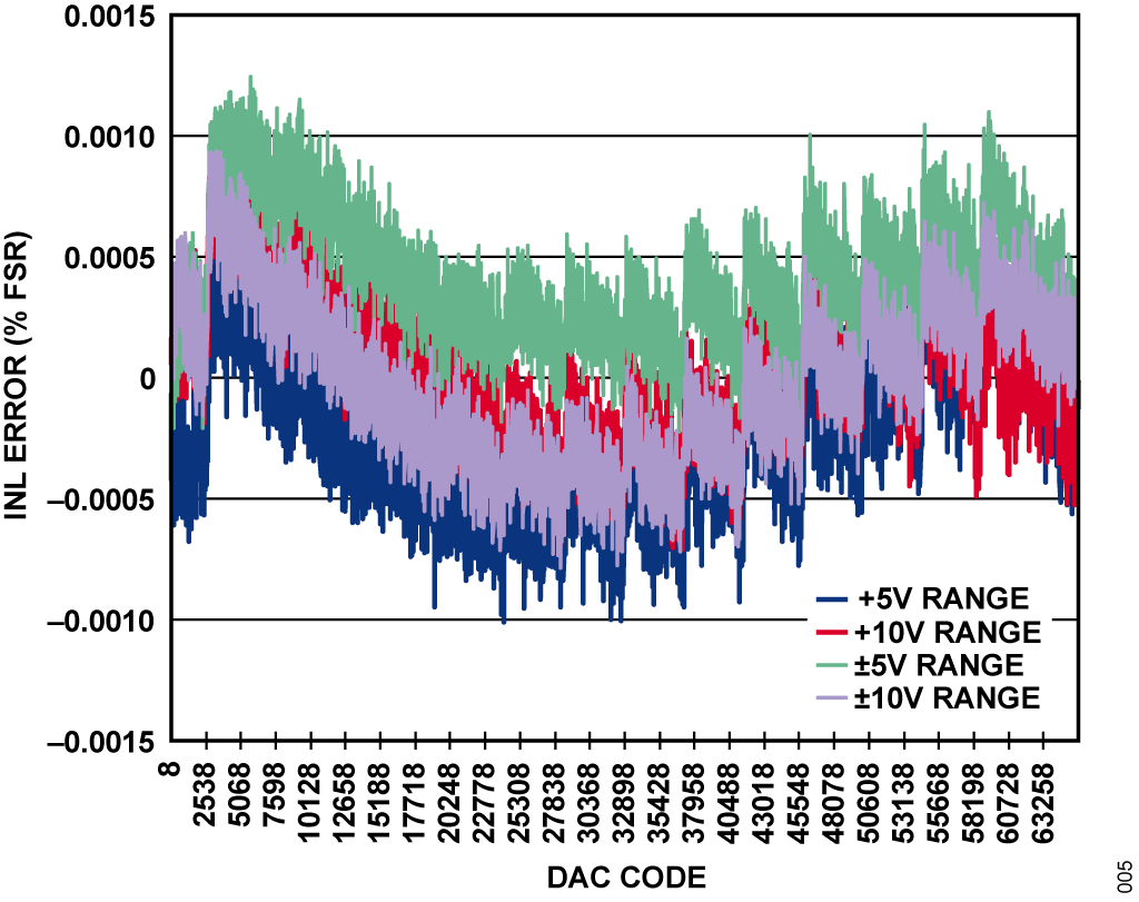
The integral nonlinearity (INL), differential nonlinearity (DNL), and total unadjusted error (TUE) of the system using the ADP2300 circuit is shown in Figure 5, Figure 6, and Figure 7, respectively. The AD5755 boost regulators were active for all the measurements.