AN-1602: 将ADuM4135栅极驱动器与Microsemi APTGT75A120T1G 1200 V IGBT模块
简介
绝缘栅极双极性晶体管(IGBT)是适用于高压应用的经济高效型解决方案,如车载充电器、非车载充电器、DC-DC快速充电器、开关模式电源(SMPS)应用。开关频率范围:直流至100 kHz。IGBT可以是单一器件,甚至是半桥器件,如为图1所示设计选择的。

本应用笔记所述设计中的APTGT75A120 IGBT是快速沟槽器件,采用Microsemi Corporation®专有的视场光阑IGBT技术。该IGBT器件还具有低拖尾电流、高达20 kHz的开关频率,以及由于对称设计,具有低杂散电感的软恢复并联二极管。选定IGBT模块的高集成度可在高频率下提供最优性能,并具有较低的结至外壳热阻。
使用ADI公司的栅极驱动技术驱动IGBT。ADuM4135栅极驱动器是一款单通道器件,在>25 V的工作电压下(VDD 至VSS),典型驱动能力为7 A源电流和灌电流。该器件具有最小100 kV/μs的共模瞬变抗扰度(CMTI)。ADuM4135可以提供高达30 V的正向电源,因此,±15 V电源足以满足此应用。
测试设置
电气设置
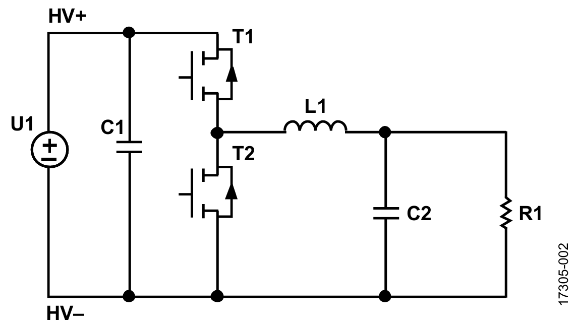
系统测试电路的电气设置如图 2 所示。直流电压施加于半桥两端的输入,900 µF (C1)的解耦电容添加到输入级。输出级为 200 µH (L1)和 50 µF (C2)的电感电容(LC)滤波器级,对输出进行滤波,传送到 2 Ω 至 30 Ω 的负载(R1)。表 1 详述了测试设置功率器件。U1 是用于 HV+和 HV−的直流电源,T1 和 T2 是单个 IGBT 模块。

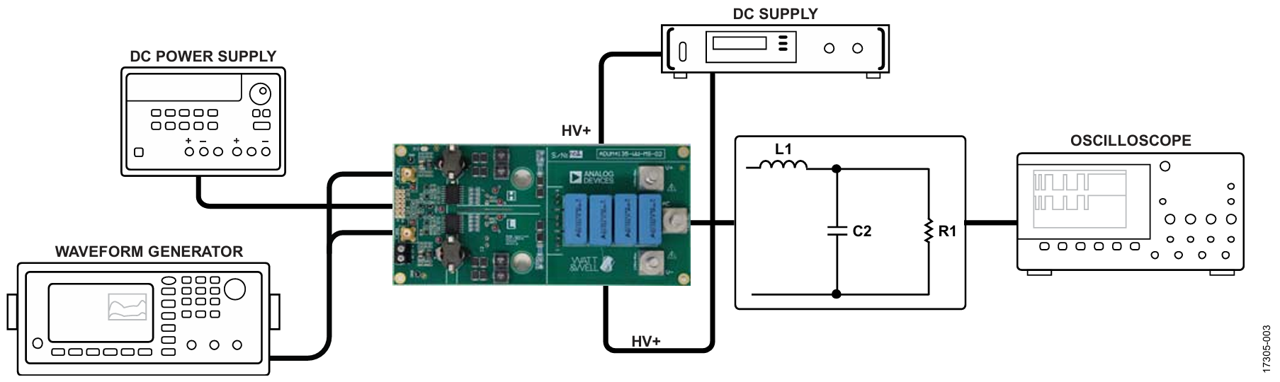
完整电气设置如图 3 所示,表 2 详细列出了测试中使用的 设备。
| 设备 | 值 |
| IGBT模块,T1,T2 | APTGT75A120T1G1 |
| U1 | 200 V至900 V |
| 电容C1 | 900 μF |
| 电感L1 | 200 μH |
| 电容C2 | 50 μF |
| 负载电阻R1 | 2 Ω至30 Ω |
| 设备 | 制造厂商 | 产品型号 |
| 示波器 | Agilent | DSO-X 3024A, 200 MHz |
| 直流电源 | Delta Elektronika | SN660-AR-11(两个串行) |
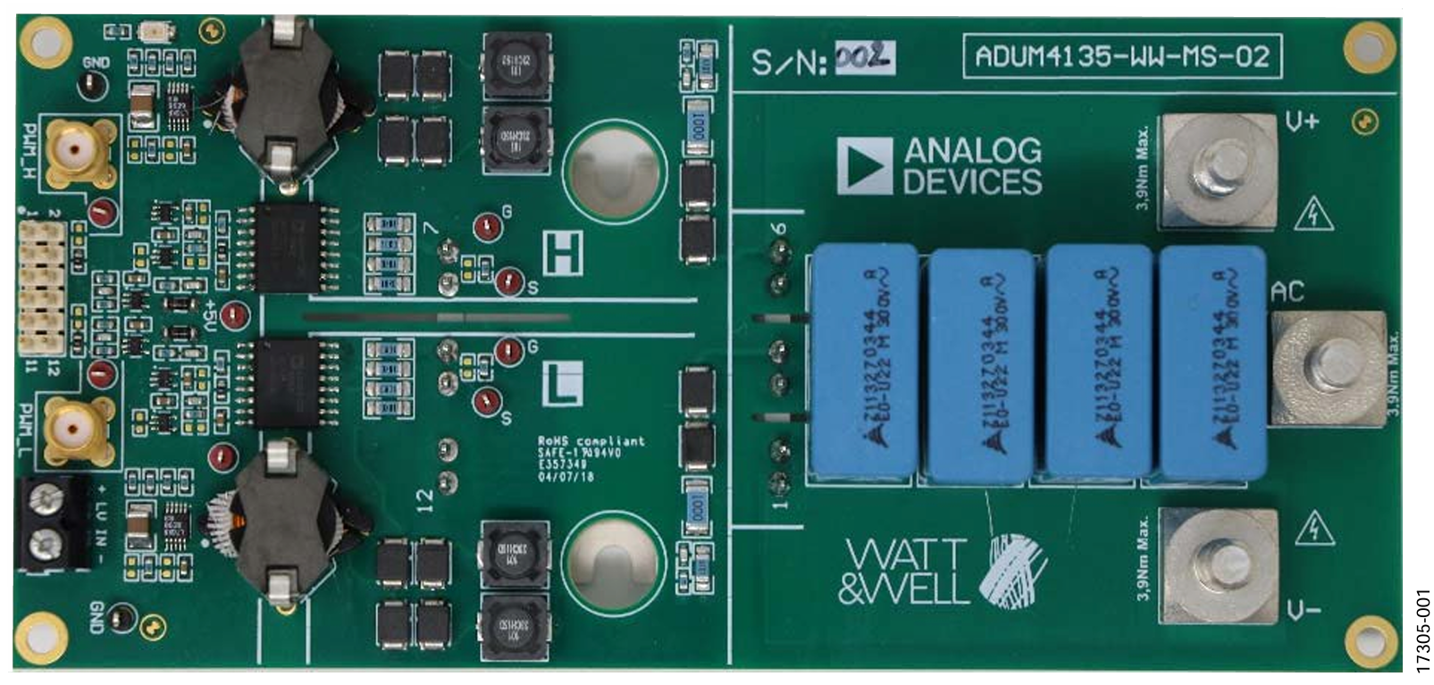
| 栅极驱动器板 | WATT&WELL | ADUM4135-WW-MS-02 SN001 |
| 波形发生器 | Agilent | 33522A |
| 电流探针 | Hioki | 3275 |
| 电流探针 | Hioki | 3276 |
| 无源电压探针 | Keysight | N2873A, 500 MHz |
| 无源高电压探针 | Elditest | GE3421, 100 MHz |
| 高压差分探针 | Tektronix | P5200 |
| 高压差分探针 | Testec | TT-SI 9110 |
| 热摄像头 | Optris | PI 160 |

测试结果
无负载测试
在无负载测试设置中,在模块输出端汲取低输出电流。在此应用中,使用一个 30 Ω 的电阻。
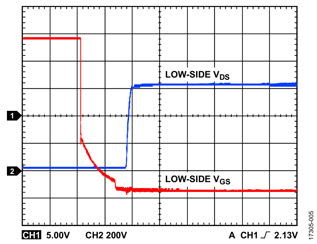
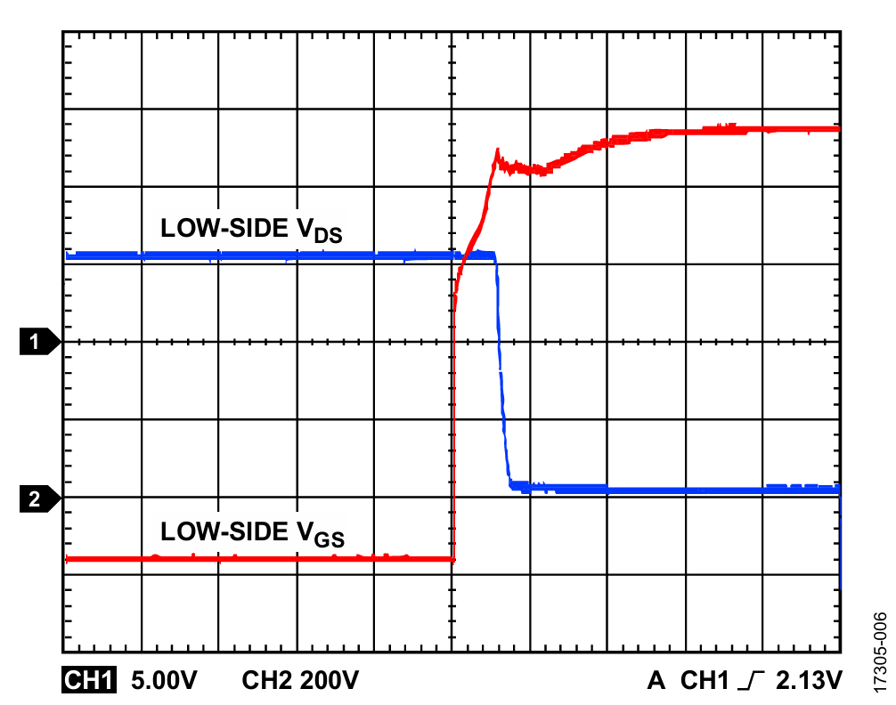
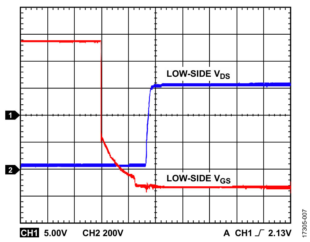
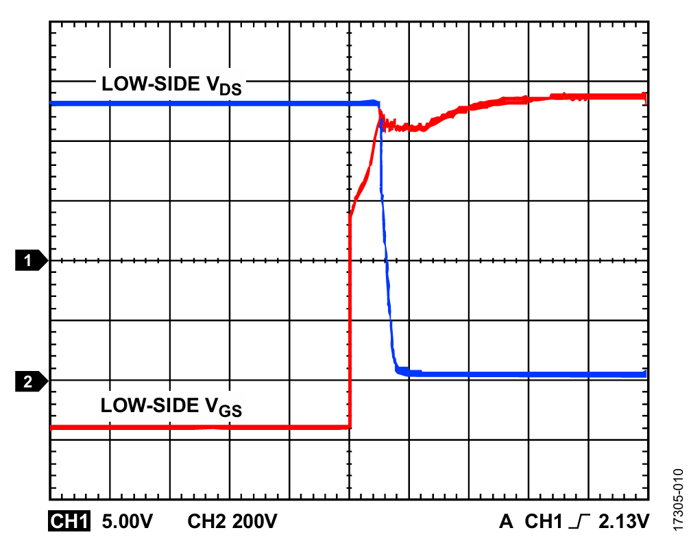
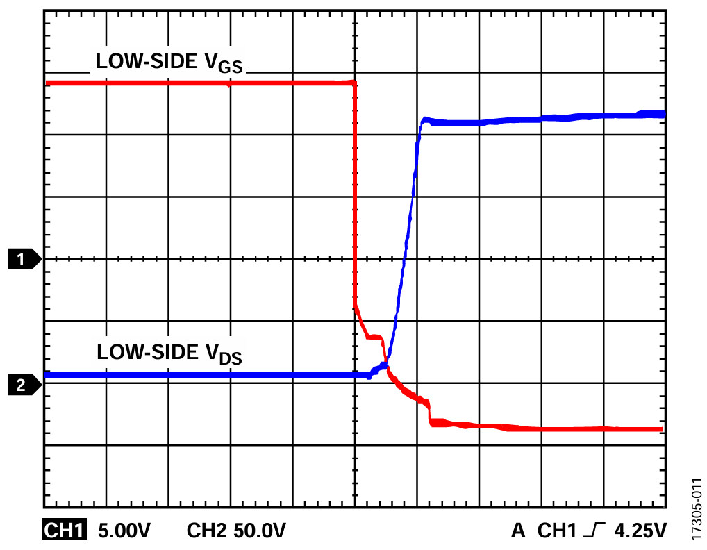
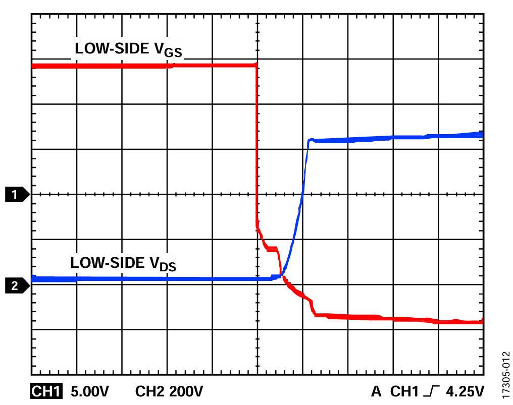
表 3 显示无负载的电气测试设置的重要元件,且负载内的电流低。表 4 显示在模块上观察到的温度。表 3 和表 4 总结了所观察到的结果。图 5 至图 10 显示各种电压和开关频率上的开关波形的测试结果。
如表 3 中所示,测试 1 和测试 2 在 600 V 电压下执行。测试 1 在 10 kHz 开关频率下执行,测试 2 在 20 kHz 开关频率下执行。测试 3 在 900 V 电压下执行,开关频率为 10 kHz。
图 4 显示无负载测试的电气设置。

| 测试 | 直流电压, VDC1, (V) | 开关频率, fSW, (kHz) | 占空比 (%) | IIN2 (A) | 参考图 |
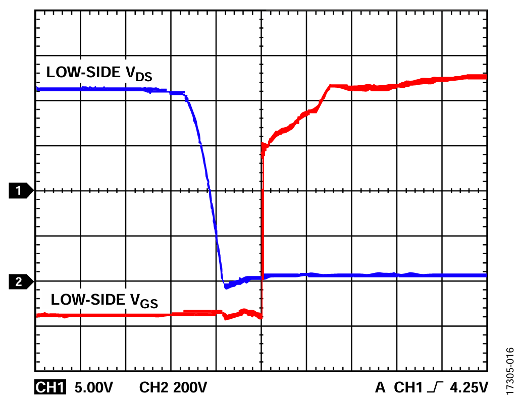
| 1 | 600 | 10 | 50 | 0.007 | 图5和图6 |
| 2 | 600 | 20 | 50 | 0.013 | 图7和图8 |
| 3 | 900 | 10 | 50 | 0.009 | 图 9 和图 10 |
1 VDC是HV+和HV−电压。
2 IIN表示通过U1的输入电流。
| 测试 | VDC (V) | fSW (kHz) | 温度 | DC-DC电源温度 | 栅极驱动器温度 | |||
| 环境(°C) | 散热器(°C) | 高边 (°C)2 | 低边 (°C)2 | 高边 (°C) | 低边 (°C) | |||
| 1 | 600 | 10 | 26 | 30.8 | 34 | 34 | 38.2 | 37.6 |
| 2 | 600 | 20 | 26 | 31 | 35 | 35 | 39.5 | 39.4 |
| 3 | 900 | 10 | 26 | 31 | 34.2 | 34.2 | 38.6 | 37.7 |
1 所有温度都通过热摄像头记录。
2 从变压器测得。
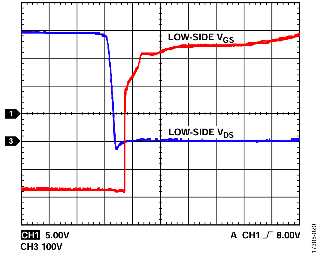
开关IGBT的性能图
此部分测试结果显示不同目标电压下的开关波形,其中 fSW = 10 kHz 和 20 kHz。VDS是漏极-源极电压,VGS是栅极-源极电压。


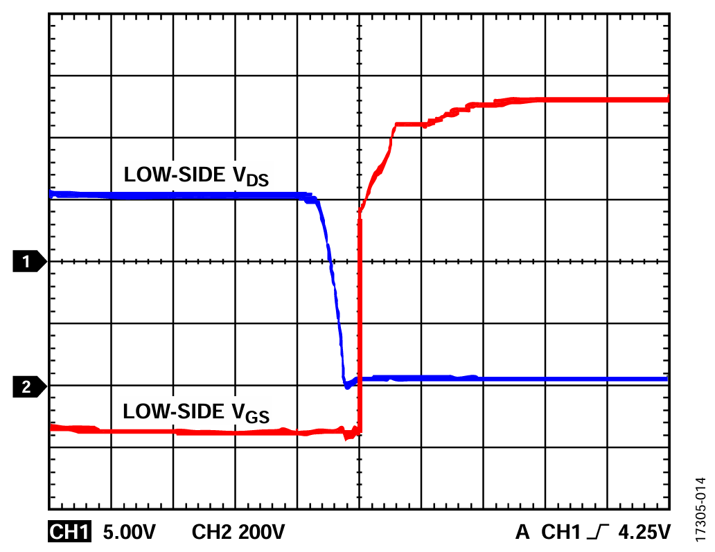
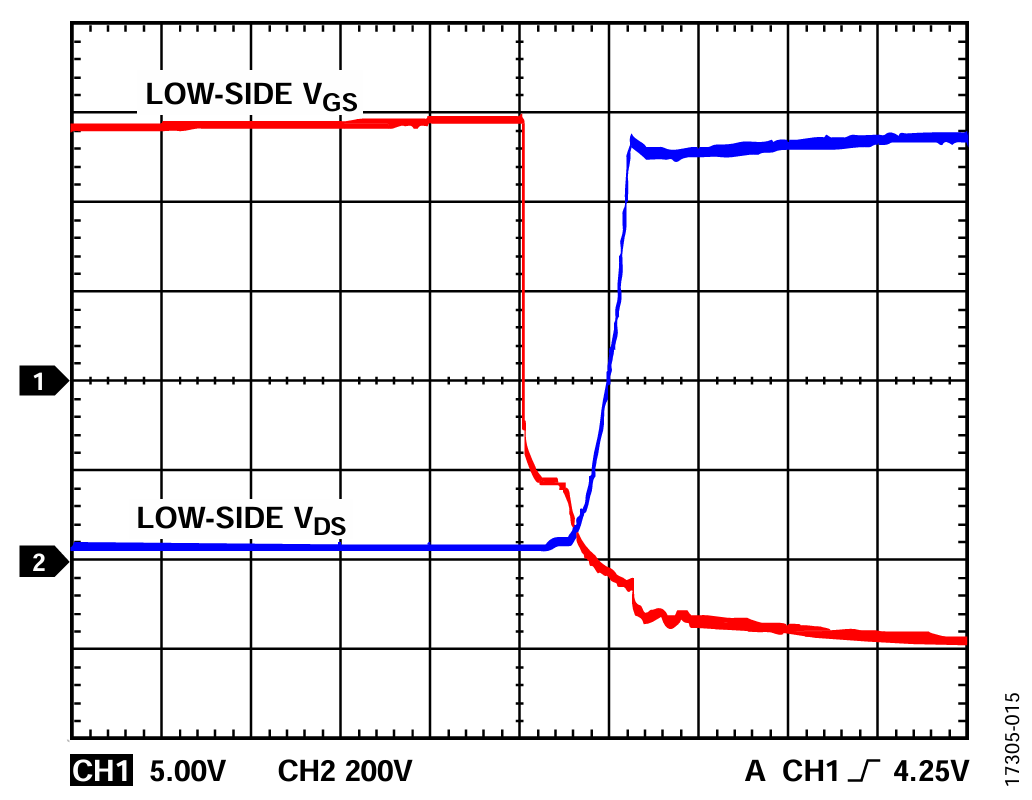
负载测试
测试配置类似于图 2 所示的测试设置。表 5 总结了观察到的结果,图 11 至图 16 显示各种电压、频率和负载下的测试性能和结果。
测试 4 在 200 V、10 kHz 开关频率下执行,占空比为 25%。
测试 5 在 600 V、10 kHz 开关频率下执行,占空比为 25%。
测试 6 在 900 V、10 kHz 开关频率下执行,占空比为 25%。
| 测试 | VDC (V) | fSW (kHz) | 占空比 (%) | IOUT1 (A) | VOUT2 (V) | POUT3 (W) | IIN (A) | 参考图 |
| 4 | 200 | 10 | 25 | 1.8 | 49.3 | 90.2 | 0.55 | 图 11 和图 13 |
| 5 | 600 | 10 | 25 | 5.4 | 146.5 | 791.1 | 1.62 | 图 12 和图 14 |
| 6 | 900 | 10 | 25 | 7.8 | 214 | 1669.2 | 2.5 | 图 15 和图 16 |
1 IOUT是负载电阻R1中的输出电流。
2 VOUT是R1两端的输出电压。
3 POUT是输出功率 (IOUT × VOUT)。
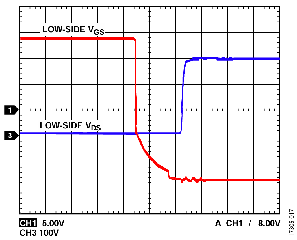
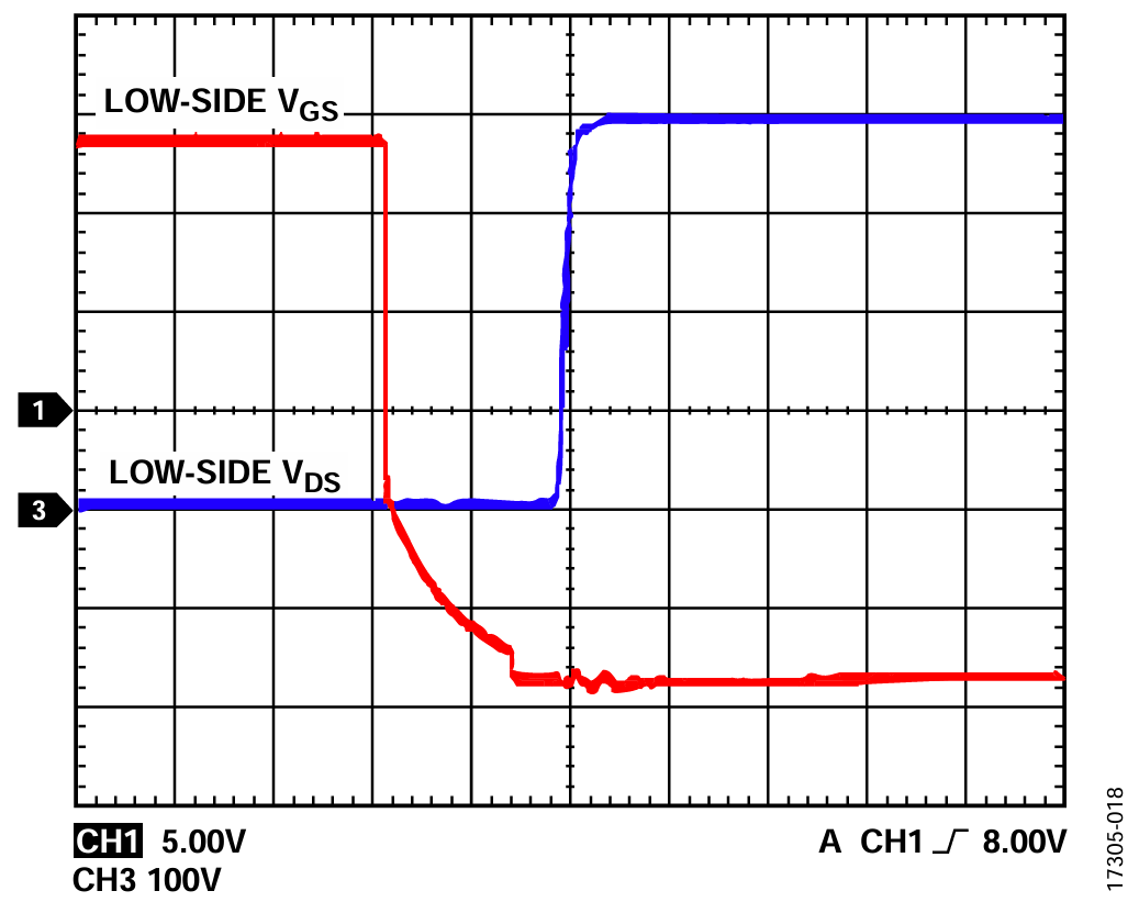
开关IGBT的性能图和无负载测试
此部分测试结果显示 fSW = 10 kHz 和 20 kHz 的不同目标电压下的开关波形。


高电流测试
测试配置类似于图3中所示的物理设置。表6总结了观察到的结果,图17至图20显示各种电压、频率和负载下的测试性能和结果。
输出负载电阻视各个测试而异,如表 1 所示,其中 2 Ω到 30 Ω 负载用于改变电流。测量 VOUT,也就是 R1 两端的电压。
测试 7 在 300 V、10 kHz 开关频率下执行,占空比为 25%。
测试 8 在 400 V、10 kHz 开关频率下执行,占空比为 25%。
| 测试 | VDC (V) | fSW (kHz) | 占空比 (%) | IOUT (A) | VOUT (V) | PIN1 (W) | IIN (A) | 参考图 |
| 7 | 300 | 10 | 25 | 19.6 | 68.7 | 1346.3 | 5 | 图 17 和图 19 |
| 8 | 400 | 10 | 25 | 25.8 | 91.7 | 2365.9 | 6.6 | 图 18 和图 20 |
1PIN 是输入电源((IIN × VIN),其中 VIN是直流电源电压。
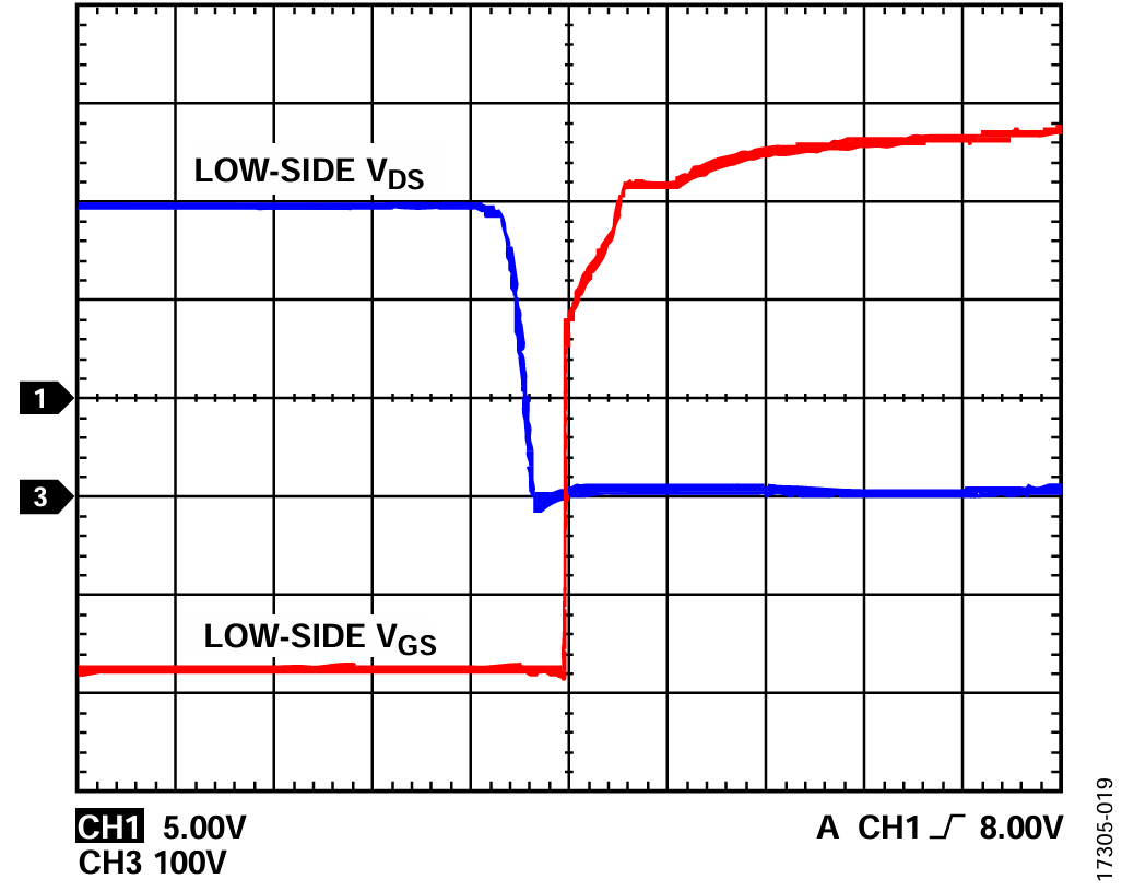
开关IGBT的性能图和负载测试
此部分测试结果显示 fSW = 10 kHz和20 kHz的不同目标电压下的开关波形。


去饱和测试
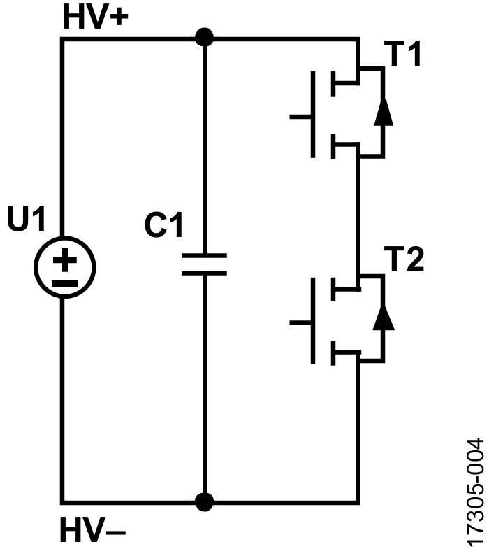
系统测试电路的电气设置如图 21 所示。直流电压施加于半桥两端的输入,900 µF 的解耦电容添加到输入级。此设置用于测试去饱和检测。在此应用中,最大 IC = 150 A,其中 IC是通过 T1 和 T2 的电流。


高端开关 IGBT (T1)被 83 μH 的电感旁路,T1 开关必须关闭。
低端开关 IGBT (T2)每 500 ms 被驱动 50 μs。
表 7 详细列出了去饱和测试设置的功率器件。
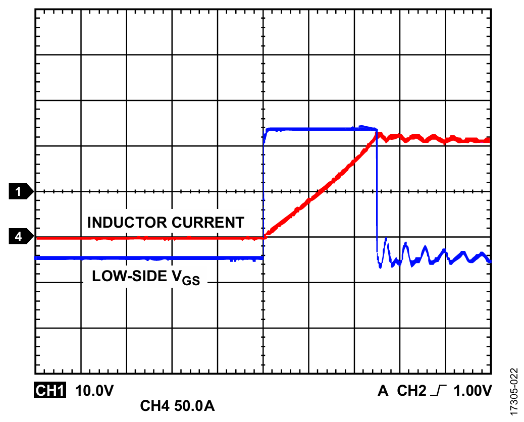
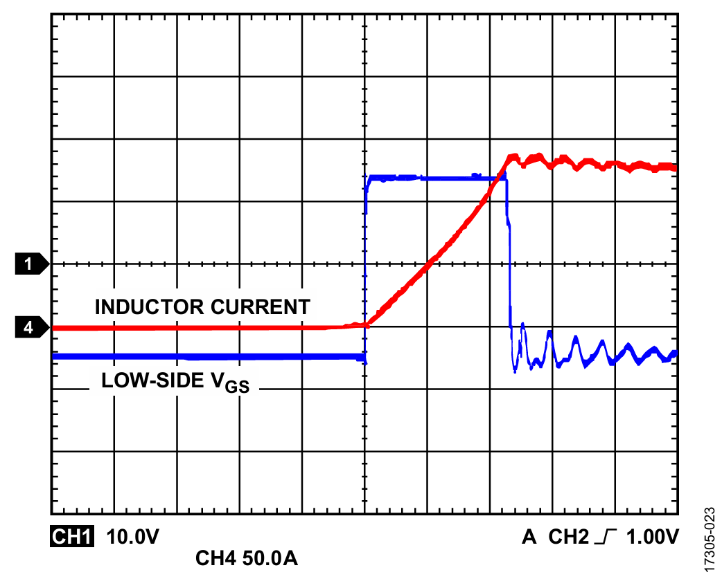
图 22 显示电感 L1 中电流 135 A 时的开关动作,图 23 显示电感 L1 中电流 139 A 时的去饱和检测。
| 设备 | 值 |
| U1 | 0 V 至 80 V |
| C1 | 900μF |
| L1 | 83 μH |


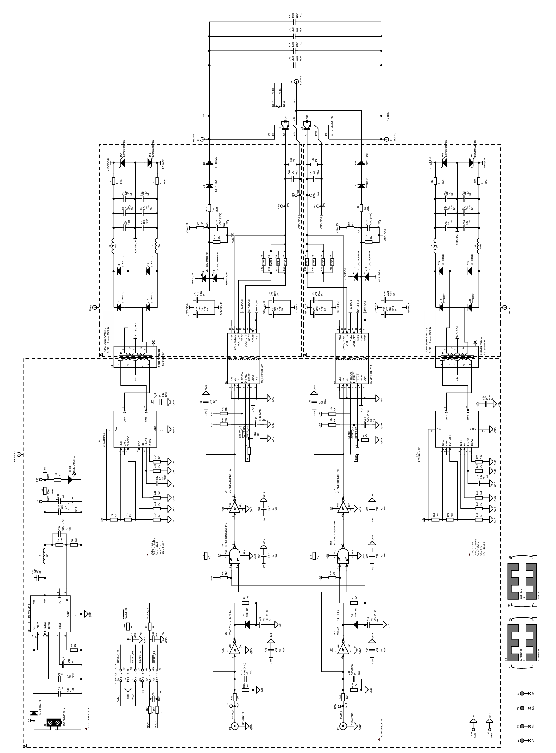
应用原理图

结论
ADuM4135栅极驱动器具有优异的电流驱动能力,合适的电源范围,还有 100 kV/µs 的强大 CMTI 能力,在驱动 IGBT时提供优良的性能。
本应用笔记中的测试结果提供的数据表明,ADuM4135评估板是驱动 IGBT 的高压应用的解决方案。
作者
