AN-0990: Terminating a Differential Amplifier in Single-Ended Input Applications
Properly terminating differential amplifiers for single-ended input applications can be challenging. This application notesimplifies the process by walking through the calculations from start to finish. The first step is to determine the input impedance of the amplifier.
Calculating The Input Impedance
The effective input impedance of a circuit depends on whether the amplifier is being driven by a single-ended or differential signal source. For balanced differential input signals, as shown in Figure 1, the input impedance (RIN, dm) between the inputs (+DIN and -DIN) is simply:
RIN, dm = 2 × RG
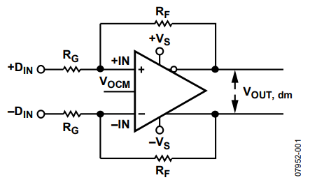
Figure 1. Differential Amplifier Configured for Balanced (Differential) Inp.
For an unbalanced, single-ended input signal (see Figure 2), calculate the input impedance using Equation 1.
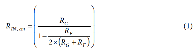
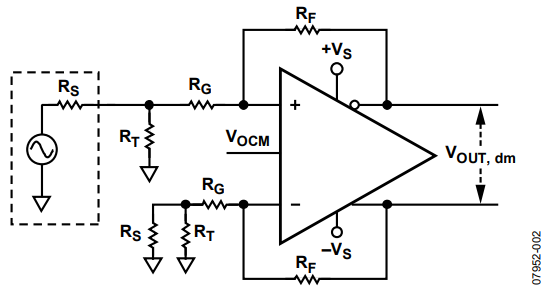
Figure 2. Differential Amplifier Configured for Unbalanced (Single-Ended) Input.
The input impedance of the circuit is effectively higher than it would be for a conventional op amp connected as an invertThis is because a fraction of the differential output voltage appears at the inputs as a common-mode signal, partialbootstrapping the voltage across the input resistor RC.
Terminating a Single-Ended Input
In this example, the circuit features an ADA4937-1, configured for unity gain. Note that this approach can be used with any differential amplifier.
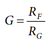
The gain of the amplifier can be calculated using the gain equation:
The Analog Devices, Inc., ADA4937-1 data sheet recommends using 200 Ω resistors. The signal source applied to the circuit is 2 V, with a source resistor of 50 Ω. The input termination can now be calculated by following these four simple steps.
-
Calculate the input impedance using Equation 1.
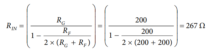
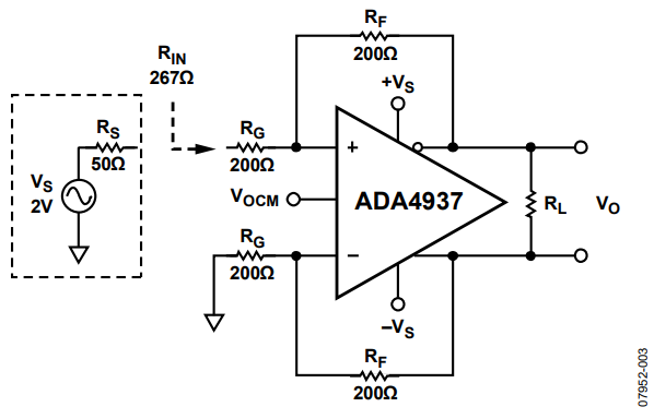
Figure 3. Single-Ended Input Impedance RIN.
-
For the source termination to be 50 Ω, calculate the termination resistor (RT) using RT||RIN = 50 Ω, which makes RT equal to 61.9 Ω.
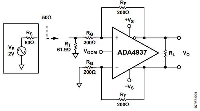
Figure 4. Adding Termination Resistor RT.
-
To compensate for the imbalance of the gain resistors, a correction resistor (RTS) is added in series with the inverting input gain resistor RG. RTS is equal to the Thevenin equivalent of the source resistance RS||RT.
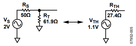
Figure 5. Calculating the Thevenin Equivalent.
RTS = RTH = RS||RT = 27.4 Ω
Note that VTH is not equal to VS/2, which would be the case if the termination were not affected by the amplifier circuit input impedance RIN.
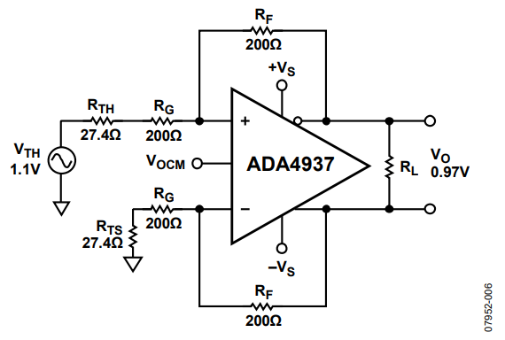
Figure 6. Balancing Gain Resistor RG.
-
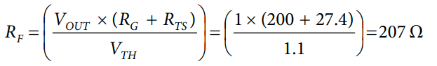
The feedback resistor must be recalculated to adjust the output voltage as shown below.
To make the output voltage VOUT = 1 V, recalculate RF using the following formula:
To make VO = VS = 2 V to recover the loss due to the input termination, RF should be:
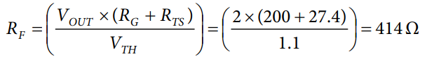
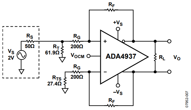
Figure 7. Complete Single-Ended-to-Differential System.
Conclusion
Calculating the input termination for a single-ended input differential amplifier is accomplished in four steps. First, calculate the amplifier input impedance RIN, then calculate the termination resistor RT. Rebalance the amplifier gain paths, by adding RTS in series with the inverting input gain resistor. Finally, calculate and adjust the feedback resistor for the correct gain. More information on differential amplifiers is available at www.analog.com.
References
作者

