Portable electronics is becoming more popular as laptop computers and telephones become smaller in size and lighter in weight. This has intensified the focus of system designers on reducing the size and the weight of the electronics in general, and power supply circuits in particular. Such considerations as board space, system cost, number of components, availability, and battery life have become increasingly important. Indeed, battery life has become a key selling feature of portable equipment, as users can expect today‘s system to operate for a much longer time than one purchased just two years ago.
Among the many applied strategies to achieve cost savings, improved efficiency and the reduction of size are the most important. The use of the latest low-dropout regulators (LDO) or fast switching regulators has reduced the loss of energy in these power supplies, leaving more energy for the rest of the system operation. New battery technologies have also served the same purpose, either reducing the size without reducing capacity, or improving capacity while retaining the same size (and weight). Standby (or sleep) modes make sense, especially when power conversion occurs locally, close to the respective loads. The system can thus switch off unused sections— such as a hard drive in a laptop computer, or the transmitter in a phone.
The newer regulators make it possible for the designer to reduce the size and overall cost of the total system solution, because they can also use smaller and less expensive external components, such as capacitors and inductors.
Simple linear voltage regulators have been around for a long time; but although they are low in cost, their dropout voltage— the minimum voltage drop across the pass transistor— is relatively high, usually between 1.5 and 3 V. The development of low-dropout regulators (LDOs), with dropout voltages as low as 0.1 V to 0.4 V per 100 mA of load current— reducing dissipation in the regulator by some 90%— was a major improvement. Besides the lower dissipation than is the case for the simple regulators mentioned above, either a lower voltage battery can be used or the battery can discharge down to a lower voltage before it needs to be replaced or recharged. This translates into longer operating time.
Low-dropout voltage regulators from Analog Devices include:
- the general-purpose ADM66x family and the ADP3367, with dropout voltage levels from 1 V down to 100 mV per 100 mA.
- a new generation of high-performance, ±0.5%-accuracy anyCAP™ LDO regulators, the ADP3300, ADP3301, and ADP3303 for 50, 100, and 250 mA full-scale output, with dropout levels of 100 or 200 mV per 100 mA.
- a dual 100-mA version of the ADP3301, the ADP3302, features the same ±0.5% accuracy and low 120-mV dropout levels.
Traditional LDOs need a bulky, expensive 10-µF load capacitor with carefully chosen equivalent series resistance (ESR); the ADP330x series can operate with a wide range of capacitor types and values— a typical example might be a 0.47 µF, low cost multilayer ceramic capacitor. This significant technology is patented and has been trade-marked “anyCAP™”.
LDOs are more efficient than conventional linear regulators and extend a battery‘s useful operating voltage, but their voltage drop wastes precious power [W = (VIN— VOUT) × IL]. All linear regulators require a higher input voltage than output voltage; they can only regulate down to the desired value, never boost up to it. So for higher efficiency, and the flexibility to have the output voltage exceed the input voltage or go negative, designers must turn to a switched-mode or a switched-capacitor regulator or converter.
By eliminating the dissipation of the pass transistor, switch-mode regulator circuits [see sidebar] can have efficiencies of 90% and more. Thus, more battery energy goes to the powered equipment, resulting in increased operating time. In obtaining high efficiency, however, switch-mode regulators also pose some challenges. For example, the need for a magnetic component increases the power supply‘s overall size and weight, both of which may be critical in portable equipment design; it also adds to the system cost.
To minimize these problems, switching frequencies are being pushed higher— up to 1 MHz in some cases— to reduce the size of inductors and capacitors. However, switching regulators have another issue: Operating in either pulse-frequency modulation (PFM) or pulsewidth modulation (PWM)1 mode, input and output ripple and electrical noise (electromagnetic interference, or EMI) are generated when the current is switched.2 Thus, depending on the application, switch-mode regulators may require filters to smooth the output ripple and/or shielding to suppress EMI. Nevertheless, the higher efficiency of switched-mode regulators has made them popular in applications such as laptop computers.
One of the switching regulators being introduced by Analog Devices is the ADP3000 (see sidebar). It can operate in boost, buck and inverter modes. In boost mode, it accepts input voltages from 2 V to 12 V, and in the buck mode, inputs up to 30 V. Fixed voltages of 3.3 V, 5 V and 12 V are offered, as is an adjustable output.
Several key features make the device well suited for portable battery-powered applications. For instance, it draws only 500 µA in the quiescent, or standby mode. The 400-kHz switching frequency means that only a small external inductor is needed. In most cases, the smallest-size inductor available (2.2 µH up to 15 µH for 1 A peak current) will suffice. Other key features are the low output voltage ripple3— less than 40 mV p-p at 3.3-V output— adjustable current limit, and an auxiliary amplifier that can serve as either a low-battery detector, linear regulator, voltage lockout or error amplifier. The example below will show how these features are used in an actual application.
Switched-capacitor voltage converters are another technique to avoid the losses associated with LDOs. An example is the recently introduced ADP3604 switched-capacitor voltage inverter with regulated output. This device delivers a regulated voltage with minimum voltage loss, very few external components, and no nductor or transformer. With a 240-kHz internal oscillator producing a 120-kHz switching frequency, the ADP3604 uses significantly smaller and cheaper capacitors than earlier designs such as the ADM660 and ADM8660. It accepts an input voltage between +4.5 V and +6.0 V and produces an output voltage of — 3 V, with ±3% accuracy and up to 120 mA of output current.
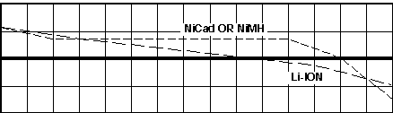
As mentioned above, battery technology has made great progress, too. Though not much used in the past, the lithium-ion (Li-ion) types become the battery of choice for many recent applications, for good reasons: They have the best energy density (ratio of charge capacity to weight), and they have long standby times, due to a very low self-discharge current. But they do have a behavior that makes them hard to use without sophisticated electronics. Their output voltage drops constantly over the time of discharge. Unlike Ni-Cd or NiMH cells, which have a lengthy plateau and then a rather sharp drop at the end of capacity (Figure 1), a Li-ion cell starts at a voltage of 4.1 V to 4.2 V (depending on the chemistry, and the specific manufacturer); then, while it is discharged, the voltage drops almost linearly all the way down to about 2.5 V. Beyond that point, since further discharge can damage the battery, it needs to be recharged.
The circuit shown in Figure 2 was designed to generate two constant 3-V outputs of up to 100 mA each from a single Li-ion cell. The output is maintained within ±1% over a range of input from 4.2 to 2.7 V, load from 0 to 100 mA per output, and operating temperature from — 40 to +85°C. The circuit has auto-shutoff to protect the battery when the input voltage has dropped to 2.5 V.
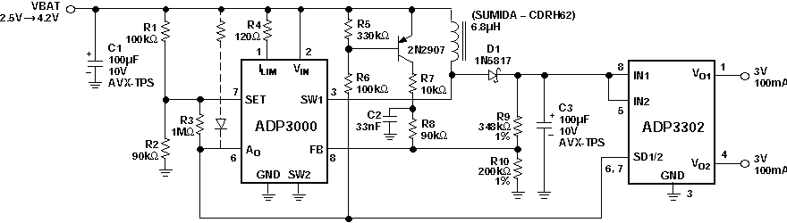
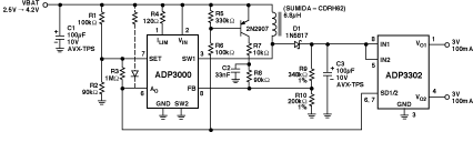
A constant +3-V output can be generated from a varying input voltage, with either an LDO or a buck-regulator (when the input is always larger than the +3-V output) or with a boost-regulator, when input is always smaller than +3 V. For the example of developing +3-V output from a single Li-ion cell over an extended life, it is necessary to provide boost when the input is less than 3.1 V, and stepdown above that voltage. There are several ways to do this. For example, an ADP1147-type stepdown switching regulator could be used in the flyback mode. The disadvantage is the ripple on both the input and the output. Or the ADP3000 could be used in a single-ended primary inductance converter circuit (SEPIC), an application shown on the data sheet, using two inductors; its weakness is rather large ripple. The ADP3000 circuit of Figure 2, with an ADP3302 dual-output LDO, is optimized to operate with smallest shielded 6.8-µH inductor to save space and money. Even smaller and cheaper are open inductors— rod types— which can be used when the environment of the power circuit is not sensitive to EMI.
Here is how the circuit works: Initially, the battery is fully charged. The input voltage is well above 3 V, and the switching regulator ADP3000 is in idle mode because the voltage at Fb (ADP3000, pin 8) is above the reference voltage (1.245 V). The LDOs (ADP3302) regulate the output voltage at 3 V. The load current (up to 2 × 100 mA) flows steadily through the inductor (resistance of 0.12 ohms), and the Schottky diode (D1) with < 0.2 V forward voltage, for a total voltage drop of about 0.23 V.
As the battery voltage decreases with time, the voltage at Fb decreases proportionally. As the input drops below about 3.7 V, the voltage at Fb goes below the 1.245-V reference voltage (voltage divider R9— R10). The internal comparator changes state, the oscillator of the ADP3000 starts; the boost converter— built up with the inductor and the diode— begins to transfer energy into capacitor C3 to keep the voltage at Fb at around 1.245 V. The lower the battery voltage drops, the more energy has to be transferred, resulting in an increasing switching frequency, that reaches well above 100 kHz just before shutdown (at 2.5 V), given a 200-mA full load4.
The SET input of the ADP3000 (pin 7) continously monitors the input voltage via the R1-R2 divider. When it falls below 2.53 V (between 2.74 V and 2.53 V, depending on the reference inside the ADP3000), Ao (Pin 6) will go to a logic LOW and shut down the ADP3302 LDO regulator by pulling SD1 & SD2 (Pins 6 & 7) to ground. At the same time, the transistor is turned on (voltage divider R5-R6) to pull Fb up and ensure that the oscillator is shut down. The remaining load current at the battery is just 500 µA from the ADP3000, plus an optional micro-LED connected to Ao as a battery depletion alarm to the user (dotted).
The 33-nF capacitor (C2) is used to filter feedthrough from the supply voltage into the sensitive feedback point, Fb. The 120-ohms resistor (R4), connected to ILIM, limits the switch current to lower the requirements for the inductor‘s current rating, at the same time reducing the output ripple and required capacitance.
The ADP3000 was designed at Analog Devices, Santa Clara, California, by James Ashe.
1PFM uses constant-on-time pulses but changes their frequency, depending on load and input voltage. This generates unpredictable interference with other system frequencies, such as system clocks, IF in telephones, etc. The frequency, starting at a few hundred Hz, will cross through the complete audio range; the problems it creates are another reason PFM technology is not well accepted in anything that contains some sort of audio. PWM uses a fixed frequency but alters the width of the pulses; its noise is therefore easier to filter.
2Switching pulses contain spikes with 20-ns to 40-ns rise times; these generate most of the EMI problems.
3Output ripple is a function of switch-peak-current × ESR (equivalent series resistance of the output capacitor). ADP3000 reduces ripple by limiting the peak current [ILIM] and using capacitors that have low ESR, such as Sony OS-COM (1.5 mΩ)]. The tantalum capacitors recommended for standard switching converters (which also lack the current-limiting feature) have ESR of about 100 mΩ.
4The oscillator runs at a constant 400ÊkHz, but a gating circuit, which lets the required number of pulses through, is responsible for the resulting frequency seen at the output.
