ADF4030
推荐新设计使用10-Channel Precision Synchronizer
- 产品模型
- 2
产品详情
- 10 BSYNC channels
- Precise BSYNC time alignment (<5 ps)
- Enables clock synchronization in large distribution networks
- Independent programmable BSYNC channel delay
- Precise path delay compensation of each BSYNC channel using bidirectional loopback capability
- Flexible physical interface supports PCB trace or cable connections with DC or AC coupling
- Each BSYNC channel supports gapped periodic clocking
- Integrated TDC
- Integrated Temperature Sensor
The ADF4030 provides for 10 bidirectional synchronized clock (BSYNC) channels and accepts a reference clock input (REFIN) signal as a frequency reference for generating an output clock on any BSYNC channels that are configured as an output. The hallmark feature of the ADF4030 is the ability to time align the clock edges of any one or more BSYNC channels to <5 ps (at the device pins) with respect to the BSYNC channel selected as the reference BSYNC channel.
The ADF4030 is well adapted for multiple connections with other ADF4030 devices for synchronizing clock signals in a system. Each BSYNC is bidirectional, allowing for reversing the direction of the clock signal to measure the propagation delay of the transmission medium. Round trip constructions that use replica paths are also supported. The bidirectional nature of the round trip delay measurement greatly reduces the error in determining the propagation delay through the BSYNC transmission medium as compared to using a replica path. This feature makes the ADF4030 capable to time align the clock edges of BSYNC channels across multiple ADF4030 devices, independent of the tree or cascade architecture in which the ADF4030 system is designed. The benefits of bidirectional clocking extend to devices other than the ADF4030 (assuming those devices support bidirectional clock exchanges).
The output divider block associated with each BYSNC channel has an optional pseudorandom binary sequence (PRBS) generator for Rev. 0 DOCUMENT FEEDBACK TECHNICAL SUPPORT FUNCTIONAL BLOCK DIAGRAM Figure 1. Functional Block Diagram producing gapped periodic clock signals that supports JESD204B and JESD204BC operation.
The ADF4030 may be used as a standalone differential time-to-digital converter (TDC) to measure the difference in time between clocks arriving at the inputs.
The RMS jitter of one ADF4030 BSYNC clock is 4.3 ps typical.
The ADF4030 is available in a 48-lead, 7 mm × 7 mm, land grid array [LGA] package and operates over the −40°C to +105°C ambient temperature range.
Throughout the data sheet, the letter x is used to mean any integer. For example, in BSYNCx, x refers to any channel from Channel 0 to Channel 9.
APPLICATIONS
- 5G timing transport high precision synchronization
- Phased array radar
- Automatic test equipment (ATE) pin electronics
- JESD204B/JESD204C support for analog-to-digital converter (ADC) and digital-to-analog converter (DAC) clocking
参考资料
ADI 始终高度重视提供符合最高质量和可靠性水平的产品。我们通过将质量和可靠性检查纳入产品和工艺设计的各个范围以及制造过程来实现这一目标。出货产品的“零缺陷”始终是我们的目标。查看我们的质量和可靠性计划和认证以了解更多信息。
| 产品型号 | 引脚/封装图-中文版 | 文档 | CAD 符号,脚注和 3D模型 |
|---|---|---|---|
| ADF4030BCCZ | 48-Terminal Land Grid Array [LGA] | ||
| ADF4030BCCZ-RL7 | 48-Terminal Land Grid Array [LGA] |
这是最新版本的数据手册
工具及仿真模型
LTspice®是一款强大高效的免费仿真软件、原理图采集和波形观测器,为改善模拟电路的仿真提供增强功能和模型。
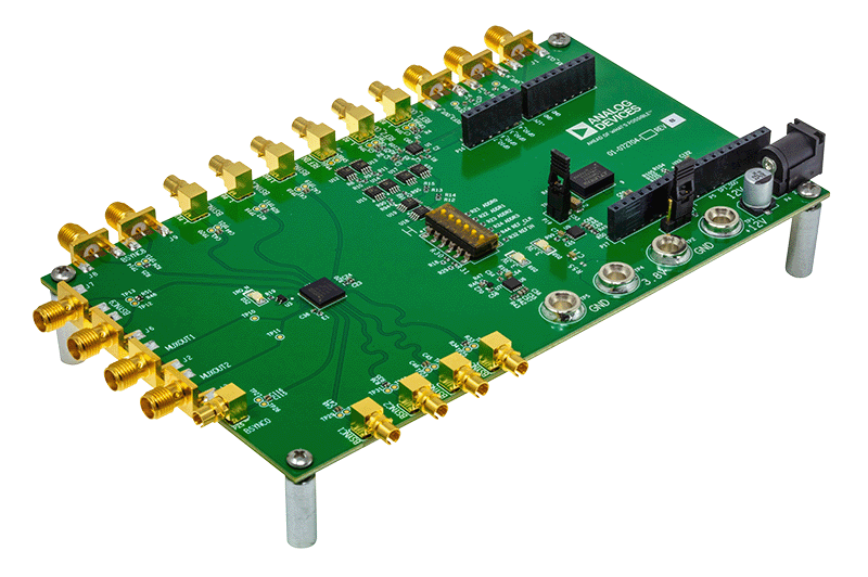
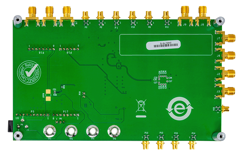
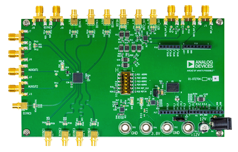
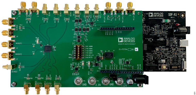
评估套件
资料
最新评论
需要发起讨论吗? 没有关于 adf4030的相关讨论?是否需要发起讨论?
在EngineerZone®上发起讨论