Q: What is a CMOS wideband switch?
A: CMOS wideband switches are designed primarily to meet the requirements of devices transmitting at ISM (industrial, scientific, and medical) band frequencies (900 MHz and up). The low insertion loss, high isolation between ports, low distortion, and low current consumption of these devices make them an excellent solution for many high frequency applications that require low power consumption and the ability to handle transmitted power up to 16 dBm. Examples of applications mentioned later in this article, include car radios, antenna switching, wireless metering, high speed filtering and data routing, home networking, power amplifiers, and PLL switching.
Q: How do these switches come to be so much faster than typical analog CMOS switches?
A: To improve their bandwidth, wideband switches use only N-channel MOSFETs in the signal path. An NMOS-only switch has a typical –3-dB bandwidth of 400 MHz—almost twice the bandwidth performance of a standard switch with NMOS and PMOS FETs in parallel. This is a result of the smaller switch size and greatly reduced parasitic capacitance due to removal of the P-channel MOSFET. N-channel MOSFETs act essentially as voltage-controlled resistors. The switches operate as follows:
Vgs > Vt → Switch ON
Vgs < Vt → Switch OFF
Where Vgs is the gate-to-source voltage and Vt is defined as the threshold voltage—above which a conducting channel is formed between the source and drain terminals.
As the signal frequency increases to greater than several hundred megahertz, parasitic capacitances tend to dominate. Therefore, achieving high isolation in the switches’ off-state and low insertion loss in the on state for wideband applications is quite a challenge for switch designers. The channel resistance of a switch must be limited to less than about 6 ohms to achieve a low-frequency insertion loss of less than 0.5 dB on a line with 50-ohm matched impedances at the source and load.
As a departure from the familiar switch topology, inserting a shunt path to ground for the off-throw—and its associated stray signal—allows the design of switches with increased off-isolation at high frequencies. The FETs have an interlocking finger layout that reduces the parasitic capacitance between the input (RFx) and the output (RFC), thereby increasing isolation at high frequencies and enhancing crosstalk rejection. For example, when MN1 is on to form the conducting path for RF1, MN2 is off and MN4 is on, shunting the parasitics at RF2 to ground, as shown in Figure 1.

Q: You mention Off Isolation and Insertion Loss. Could you explain what these are?
A: Yes, the two most important parameters that describe the performance of an RF switch are the insertion loss in the closed state and the isolation in the open state.
Off isolation is defined as the attenuation between input and output ports of the switch when the switch is off. Crosstalk is a measure of the isolation from channel to channel.
For example, the ADG919 SPDT switch provides about 37 dB of isolation at 1 GHz, as shown in Figure 2. The same device, using the chip-scale package (CSP)—offered for space-constrained wireless applications, such as antenna switching—offers a 6-dB improvement (43 dB at 1 GHz).

Insertion loss is the attenuation between input and output ports of the switch when the switch is on. The switch is generally one of the first components encountered in a receiver’s signal path, so a low insertion loss is required to ensure minimum signal loss. Low switch insertion loss is also important for systems that require a low overall noise figure.
To obtain the best insertion-loss performance from the ADG9xx family of switches, one should operate the part at the maximum allowable supply voltage of 2.75 V. The reason can be seen in Figure 3, which shows plots of insertion loss versus frequency for the ADG919 at three different values of supply voltage.

Q: How does insertion loss relate to the On-resistance spec of a standard analog switch?
A: Signal loss is essentially determined by the attenuation introduced by switch resistance in the on condition, Ron, in series with the source-plus-load resistance—measured at the lower frequencies of operation. Figure 4 shows a typical profile of on-resistance as a function of source voltage for an N-channel MOSFET device.

Q: What technologies have been commonly used in the design of high-frequency switches?
A: Traditionally, only a few processes were available for developing good wideband/RF switches. Gallium arsenide (GaAs) FETs, PIN diodes, and electromechanical relays have dominated the market, but standard CMOS is now a strong entry.
PIN diodes are highly linear devices with good distortion characteristics, but they have many drawbacks given today’s high performance demands. They have very slow switching times (microseconds, compared to nanoseconds for CMOS switches); they are power-hungry, making them unsuitable for many battery-operated devices; and—unlike CMOS switches with their response from RF to dc—there is a practical lower frequency limit to the use of PIN diodes as linear switches.
GaAs has been popular because of its low on resistance, low off capacitance, and high linearity at high frequencies. As CMOS process geometries continue to shrink, however, the performance of CMOS switches has increased to the extent that they can achieve –3-dB frequencies of up to 4 GHz and are able to compete with GaAs switches. Designed to maximize bandwidth while maintaining high linearity and low power consumption, CMOS switches now offer a practical alternative to GaAs switches in many low-power applications.
Q: So what are the main benefits of CMOS wideband switch solutions over gallium arsenide?
A: Switches, such as the ADG9xx family of parts, have an integrated TTL driver that allows easy interfacing with other CMOS devices, since CMOS is compatible with LVTTL logic levels. The small size of devices with integrated drivers is a solution for many space-constrained applications.
GaAs switches, as such, need dc-blocking capacitors in series with the RF ports, effectively floating the die relative to dc ground, so that the switches can be controlled with positive control voltages. Wideband switches, such as the ADG9xx family, do not have this requirement, eliminating concerns of reduced bandwidth, the impact of the capacitors on overall system performance, and the extra space and cost of GaAs solutions. Eliminating the blocking capacitors allows the ADG9xx parts to maintain their low insertion loss (0.5 dB) all the way down to dc. In addition to providing a smaller, more efficient design solution, the ADG9xx family is less power-demanding, consuming less than 1 μA over all voltage and temperature conditions.
Q: How about the ESD (electrostatic discharge) performance as compared to GaAs?
A: The ADG9xx family of parts passes the 1-kV ESD HBM (human body model) requirement. ESD protection circuitry is easily integrated on these CMOS devices to protect the RF and digital pins. This makes the switches ideal for any applications that are ESD sensitive, and they offer a reliable alternative to GaAs devices having ESD ratings as low as 200 V.
Q: What are the other important specifications of these switches?
A: Video Feedthrough (Figure 5) is the spurious dc transient present at the RF ports of the switch when the control voltage is switched from high- to- low-, or low- to- high, without an RF signal present. This is analogous to charge injection of a typical analog switch. It is measured in a 50-ohm test setup, with 1-ns (rise-time) pulses and a 500-MHz bandwidth.

P1dB (1-dB compression point) is the RF input power level at which the switch insertion loss increases by 1 dB over its low-level value. It is a measure of the RF power-handling capability of the switch. As shown in Figure 6, the ADG918 has a P1dB of 17 dBm at 1 GHz, with VDD = 2.5 V.
Q: What does this mean?
A: It means that if the insertion loss at 1 GHz was 0.8 dB with a low-level input, it would be 1.8 dB with a 17-dBm input signal [Note: dBm is the dB (logarithmic) measure of the ratio of power to 1 mW, or voltage to 224 mV in 50 ohms. 17 dBm corresponds to 50 mW, or 1.6 V rms or 4.5 V p-p].

Q: Power-handling capability seems to decrease substantially at the lowest frequencies in Figure 6. Why?
A: In normal operation, the switches can handle a 7-dBm (5-mW) input signal. For a 50-ohm load, this corresponds to a 0.5-V rms signal, or 1.4 V peak-to-peak for sine waves. [V p-p = Vrms × 2 × √2].
The power handling capability is reduced at lower frequencies for two reasons:
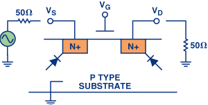
As shown in Figure 7, the inherent NMOS structure consists of two regions of N-type material in a P-type substrate. Parasitic diodes are thus formed between the N and P regions. When an ac signal, biased at 0 V dc, is applied to the source of the transistor, and Vgs is large enough to turn the transistor on (Vgs > Vt), the parasitic diodes can be forward-biased for some portion of the negative half-cycle of the input waveform. This happens if the input sine wave goes below approximately –0.6 V, and the diode begins to turn on, thereby causing the input signal to be clipped (compressed), as shown in Figure 8. The plot shows a 100-MHz, 10-dBm input signal and the corresponding 100-MHz output signal. It is readily seen that the output signal has been truncated.

At low frequencies, the input signal is below the –0.6 V level for longer periods of time, and this has a greater impact on the 1-dB compression point (P1dB).
The second reason why parts can handle less power at lower frequencies is the partial turn-on of the shunt NMOS device when it is supposed to be off. This is very similar to the mechanism described above where there was partial turn-on of the parasitic diode. In this case, the NMOS transistor is in the off state, with Vgs < Vt. With an ac signal on the source of the shunt device, there will be a time in the negative half-cycle of the waveform where Vgs > Vt, thereby partially turning on the shunt device. This will compress the input waveform by shunting some of its energy to ground.
Both of the above mechanisms can be overcome by applying a small dc bias (about 0.5 V) to the RF input signal when the switch is being used at low frequencies (<30 MHz) and high power—greater than 7 dBm (or 5 mW, 1.4 V p-p in 50 ohms). This will raise the minimum level of the sine-wave input signal and thus ensure that the parasitic diodes are continually reverse-biased and that the shunt transistor, never seeing Vgs > Vt, remains in the off state for the whole period of the input signal. Figure 9 again shows a plot of input- and output signals at 100 MHz and 10 dBm input power (about 2 V p-p in 50 ohms), but this time with a 0.5-V dc bias. It is clearly visible that clipping or compression no longer occurs at 100 MHz.

Q: How do I apply a dc bias to RF inputs?
A: To minimize any current drain through the termination resistance on the input side, it is best to add the bias on the output (RFC) side. This is the best practice, especially for low-power portable applications, but it may be necessary to apply dc-blocking capacitors on the RF outputs if downstream circuitry cannot handle the dc bias.
Q: Can these switches operate with a negative supply?
A: They can operate with a negative signal on the GND (ground) pin as long as it adheres to the –0.5 V to +4 V Absolute Maximum Rating for VDD to GND. Note that operating the part in this manner places the internal terminations at this new GND potential—an undesirable effect in some applications.
Q: What about the distortion performance of these switches?
A: When tones at closely spaced frequencies are passed through a switch, the nonlinearity of the switch causes false tones to be generated, causing undesired outputs at other frequencies. In communications systems, where channels are becoming more tightly spaced, it is essential to minimize this intermodulation distortion (IMD) to ensure minimum interference. Applying two closely spaced equal-power signals with a set frequency spacing (e.g., 900 MHz and 901 MHz) to the input of a device under test (DUT), results in the output spectrum shown in Figure 10. The 3rd-order harmonic, usually expressed in dBc, is the log of the ratio of the power in the 3rd order harmonic to the power of the fundamental. The larger the (negative) value, the lower the distortion. Sending these tones through the ADG918, using a combiner with an input power of 4 dBm, resulted in an IP3 of 35 dBm as shown in Figure 11. [Note: an excellent discussion of various types of distortion can be found in “Ask The Applications Engineer—13”]


IP3—Third-order intercept point. The IMD is measured, and from this the IP3 value is calculated. IP3 is a figure of merit—in dBm—for the device. IP3, specified in the data sheet, is a measure of the distortion caused by the switch due to the power in these false tones. The larger the IP3 value the smaller the tones in the adjacent channels, indicating that the switch has good harmonic performance.
Q: What configurations are available in the ADG9xx family?
A: The ADG9xx family comprises SPST (single-pole, single-throw), SPDT (single-pole, double-throw), and dual-SPDT switches—and 4:1 single-pole multiplexers (SP4T). These are offered in both absorptive and reflective versions, in order to suit all application needs.
Q: What is an absorptive switch?
A: The ADG901 (SPST), ADG918 (SPDT), ADG936 (dual SPDT), and the ADG904 (SP4T) parts are described as absorptive (matched) switches, because they have on-chip 50-ohm-terminated shunt legs.

Q: What is a reflective switch?
A: The ADG902 (SPST), ADG919 (SPDT), ADG936-R (dual SPDT), and the ADG904-R (SP4T) parts are described as reflective switches because they have 0-ohm shunts to ground.
Q: Where would I use an absorptive switch over a reflective switch?
A: An absorptive switch has a good impedance-match, or voltage standing-wave ratio (VSWR), on each port, regardless of the switch mode. It should be used when there is a need for proper back-termination in the off channel, to maintain a good VSWR. An absorptive switch is therefore ideal for applications that require minimum reflections back to the RF source. It also ensures that the maximum power is transferred to the load in a 50-ohm system.
A reflective switch is suitable for applications where high off-port VSWR does not matter and the switch has some other desired performance feature. Reflective switches are commonly used in applications where the matching is provided elsewhere in the system. In most cases, an absorptive switch can be used instead of a reflective switch, but not vice versa.
Q: How can I determine the VSWR of these switches?
A: VSWR—voltage standing-wave ratio—the ratio of the sum of forward and reflected voltages to the difference of forward and reflected voltages—indicates the degree of impedance match present at the switch RF port. When it comes to measurement, it is easier to describe the impedance match in terms of return loss, the amount of reflected power relative to the incident power at a port.
Simply by measuring both incident and reflected power, the return loss can be determined, and from this the VSWR can be calculated by using readily available VSWR/return-loss conversion charts. Figure 13 shows a typical return-loss curve for the ADG918 in the on- and off conditions. Note that the ADG918, an absorptive switch, has good return-loss performance for the off, as well as the on, switch. The ADG919 version, which does not include termination resistors, would not have good return-loss performance in the off condition.

Q: Now that you’ve explained how these parts perform, tell me where and how they are used.
A: Due to their low insertion loss at up to 1-GHz and wide –3-dB bandwidth (up to 4 GHz), switches in this family are ideal for many automotive entertainment systems.
They have found homes in tuner modules and set-top boxes to switch between the cable-TV input and the off-air antenna input. Another area where these parts are suitable is in car-radio antenna switching. Because these are generally 50-ohm-impedance systems, the 50-ohm internal terminations offered by the absorptive version of these switches—the ADG901, ADG918, and ADG904—ensure excellent impedance-matching and minimum reflections.
The variety of topologies available makes these parts very easy to design into antenna-diversity-switch applications, allowing the user to switch between several antennas and a single tuner in multiband radios.
These parts are also suitable for wireless metering systems, providing the required isolation between transmit and receive signals (Figure 14).

These parts are perfect for high-speed filter selection and data routing: the ADG904 can be used as a 4:1 demultiplexer to switch high-frequency signals between different filters—and also to multiplex the signal to the output. For differential filter selection and data routing, the ADG936 dual SPDT (single-pole, double-throw) switch is an ideal solution. Data switching in modem cards for point-to-point wireless systems, such as microwave radio links for military and avionic applications, requires the high-frequency performance offered by the ADG9xx family of parts.
They are also suitable for home-networking applications—systems allowing the wireless remote control of many different functions, such as opening and closing roller blinds, control of lighting (on, off or dimming)—in which the information is transmitted through a wireless link. The excellent isolation performance at high frequency and low power-consumption preserve a system’s current budget—thus constituting an ideal application.
Due to their high frequency range—up to 4 GHz—this family of parts are also suitable for many Bluetooth technologies—enabling wireless communication in the 2.5-GHz ISM frequency band.
Wideband switches can be used in the design of power amplifiers (PAs) with 800-, 900-, 1900-, 2100-MHz frequencies—for cellular CDMA and GSM applications. The switch is used in the feed forward correction loop around the main amplifier, allowing the active- and passive feedback- and feed-forward paths to be switched out, permitting the amplifier’s distortion levels to be tested. The switch allows for gain- and phase correction in the system. The high isolation, low insertion loss, and the low distortion at 900 MHz make the ADG9xx family ideal for PA design in this frequency range.
The ADG918 can be used to implement PLL switching for frequency-hopping in GSM applications.
Q: What is PLL Switching, and why use the ADG918?
A: Switching between two phase-locked loops (PLLs)—commonly described as the ping-pong technique—allows a designer to achieve faster system settling times. The low power-consumption and simple single-pin control of the ADG918 make it an easy solution to integrate.
In switching between two oscillators, the desired isolation performance can be achieved by cascading—i.e., connecting a number of switches in cascade. This is a very simple way to provide a high-isolation specification for a system, preventing any interference at the higher frequencies. Cascading five ADG918s provides 130-dB isolation at 1 GHz, with an insertion loss of 3 dB. In this application, such an increase in insertion loss is not material, since the principal concern is about the signal levels relative to one another.
A nice feature of the ADG918 in this application is that it acts as an integrated low-pass filter, eliminating the unwanted harmonics created by the two PLLs. Achieved by the natural increase in insertion loss at high frequencies, it easily prevents the unwanted harmonics from propagating through the switches, as shown in Figures 15 and 16.


Q: So...to summarize?
A: In summary, CMOS wideband switches, especially those in the ADG9xx family, are excellent choices for all applications in the ISM band that require high isolation and low insertion-loss for battery-operated devices with space constraints. Evaluation kits are available from Analog Devices to make the design-in of these parts fast and hassle free—every designer’s dream!
