Designed on small-geometry processes, high-performance ADCs typically run on a single 1.8-V to 5-V supply or dual ±5-V supplies. To process real-world signals of ±10 V or larger, the ADC is often preceded by an amplifier that attenuates the signal to keep it from saturating or damaging the ADC inputs. These amplifiers usually have single-ended outputs, but differential outputs would be preferable to capture the full benefits of the differential-input ADC, including increased dynamic range, improved common-mode rejection, and reduced noise sensitivity. Figure 1 shows a differential-output amplifier system with gain of 1/2.
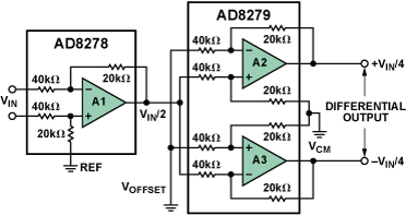
Differential amplifier A1 is configured for a gain of 1/2. The output of this amplifier is fed into the noninverting input of amplifier A2 and the inverting input of amplifier A3. Amplifiers A2 and A3 also operate at a gain of 1/2. Their outputs, 180 degrees out of phase, form a differential output. The differential output voltage, VOUT A2 – VOUT A3, is equal to VIN/4 – (–VIN/4), or a total differential output voltage of VIN/2, as desired.
The VOFFSET terminal can be used to offset the output and increase the dynamic range of the ADC. The differential gain from VOFFSET to the output is –1. Connect this node to ground if offset adjustment is not required.
The VCM terminal sets the common-mode voltage of the differential output. This is particularly useful when driving single-supply ADCs, as the common-mode output of the circuit can be set to midsupply. The gain from VCM to the output is 1. Connect this node to ground if common-mode adjustment is not required.
Figure 2 demonstrates the circuit's performance. The input is a 25-kHz, 20-V p-p sine wave. Channel 1 is the noninverting output; Channel 2 is the inverting output; Channel 3 is the input. The Math Channel is the difference between the two outputs. Each output is 1/4 of the input signal; the two outputs are inverted with respect to each other; and their difference is 1/2 of the input signal.
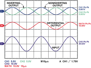
Figure 3 shows the gain vs. frequency response of the circuit, demonstrating that it is stable, with less than 1-dB peaking over a 1-MHz bandwidth.
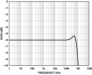
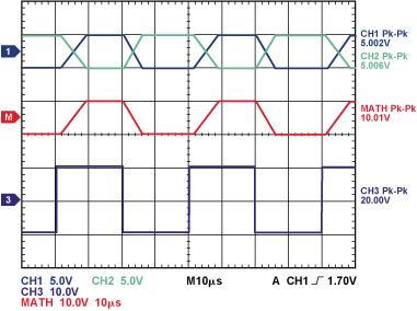
Figure 4 demonstrates that the circuit's response to large square-wave inputs has no appreciable overshoot and a quick settling time. The differential output slews twice as fast as the individual outputs because each amplifier carries only half of the signal.
The AD8279 dual difference amplifier is available in a narrow-body 14-lead SOIC package. The AD8278 is available in an 8-lead MSOP package. Because the precision laser-trimmed resistors are integrated onto the same chip as the amplifiers, their offset, gain, common-mode errors—and drift over temperature—are minimized, making for a high-precision system. Despite the low power consumption of the AD8278 (200 µA) and AD8279 (200 µA per amplifier), the system has a 1-MHz bandwidth and a 2.4-V/µs slew rate. The AD8278 and AD8279 can operate over a very large supply voltage range, from a single 2.5-V supply to dual ±18-V supplies. The inputs can swing well beyond the supply rails, enabling them to measure large signals (±20 V or more) in the presence of large common-mode voltages and noise, making this an ideal front end for high-performance, low-voltage ADCs.

