Introduction
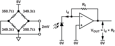
The need to measure signals with a wide dynamic range is quite common in the electronics industry, but current technology often has difficulty meeting actual system requirements. Weigh-scale systems typically use load-cell bridge sensors with maximum full-scale outputs of 1 mV to 2 mV. Such systems may require resolutions on the order of 1,000,000 to 1, which, when referred to a 2-mV input, call for a high-performance, low-noise, high-gain amplifier and a Σ-∆ modulator. Similarly, chemical and blood analysis for medical applications often use photodiode sensors, producing very small currents that need to be accurately measured (see Figure 1). A low-noise transimpedance amplifier is typically used, with multiple stages of gain and post processing.
While the actual sensor data typically takes up only a small portion of the input signal range, the system must often be designed to handle fault conditions. Thus, a wide dynamic range, high performance with small inputs, and quick response to fast-changing signals, are key requirements. Some applications, such as vibration-monitoring systems, contain both ac and dc information, so the ability to accurately monitor both small and large signals is growing in importance.
These requirements call for a flexible signal-conditioning block, with low-noise inputs, relatively high gains, and the ability to dynamically change the gain in response to input level changes without affecting performance, while still maintaining a wide dynamic range. Existing Σ-∆ technology can provide the dynamic range needed for many applications, but only at the expense of update rate. This article presents an alternative approach that uses a high-speed, successive-approximation, sampling ADC, combined with an autoranging programmable-gain amplifier (PGA) front end. With gain that changes automatically based on analog input value, it uses oversampling to increase the dynamic range of the system to more than 126 dB.
Technology
In ADC applications, dynamic range is the ratio of the rms value of the full scale to the rms noise, which is generally measured with the analog inputs shorted together. Commonly expressed in decibels (dBV = 20 × log10 of the voltage ratio), it indicates the range of signal amplitudes that the ADC can resolve; an ADC with a dynamic range of 60 dB can resolve signal amplitudes with a range of 1000:1. For an N-bit ADC, the dynamic range (DR) can be calculated as:
DR = 6.021N + 1.763 dB
The Σ-∆ ADCs, such as the AD7767, achieve excellent dynamic range by combining a Σ-∆ modulator with a digital postprocessor. The digital filtering that follows the converter acts to remove the out-of-band quantization noise, but it also reduces the data rate from fMCLK, at the input of the filter, to fMCLK/8, fMCLK/16, or fMCLK/32, at the digital output—depending on which model of the device is being used. For increased dynamic range, a low-noise PGA can be added to condition the input signal to attain full scale. The noise floor of the system will be dominated by the input noise of the front-end PGA—depending on the gain setting. If the signal is too large, it overranges the ADC input. If the signal is too small, it gets lost in the converter’s quantization noise. The Σ-∆ ADCs often tend to be used for applications that require lower system update rates.
Oversampling Successive-Approximation ADC to Improve Dynamic Range
One method for increasing the dynamic range of a successive-approximation ADC is to implement oversampling: the process of sampling the input signal at a much higher rate than the Nyquist frequency. As a general rule, every doubling of the sampling frequency yields approximately a 3-dB improvement in noise performance (see Figure 2). Oversampling can be implemented digitally using post-processing techniques. Some ADCs, such as the AD7606, have programmable oversampling rates, enabling the end user to choose the appropriate oversampling ratio.

Combining PGA Functionality with Oversampling
To achieve maximum dynamic range, a front-end PGA stage can be added to increase the effective signal-to-noise ratio (SNR) for very small signal inputs. Consider a system dynamic range requirement of >126 dB. First, calculate the minimum rms noise to achieve this dynamic range. For example, a 3-V input range (6 V p-p) has a 2.12-V full-scale rms value (6/2√2). The maximum allowable system noise is calculated as
126 dB = 20 log (2.12 V/rms noise)
Thus, the rms noise ≈ 1 µV rms.
Now, consider the system update rate, which will determine the oversampling ratio and the maximum amount of noise, referred to the input (RTI), that can be tolerated in the system. For example, with the AD7985 16-bit, 2.5-MSPS PulSAR® ADC running at 600 kSPS (11 mW dissipation) and an oversampling ratio of 72, the input signal is limited to a bandwidth of approximately 4 kHz. The total rms noise is simply the noise density (ND) times √f, so the maximum allowable input spectral noise density (ND) can be calculated as
1 μV rms = ND × √4 kHz
Or, ND = 15.5 nV/√Hz
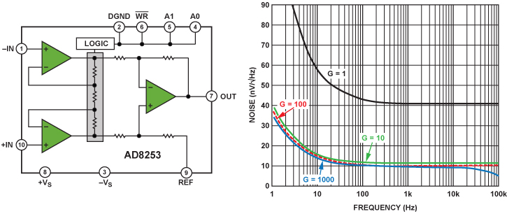
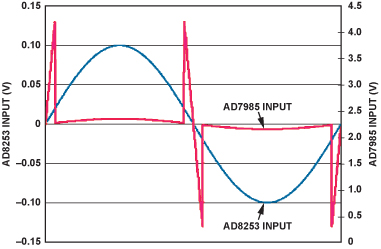
From this figure of merit for RTI system input noise, a suitable instrumentation amplifier can be chosen that will provide sufficient analog front-end gain (when summed with the SNR of the ADC, with associated oversampling) to achieve the required 126 dB. For the AD7985, the typical SNR figure is 89 dB, and oversampling by 72 yields another ~18-dB improvement (72 is approximately 26, and each doubling adds 3 dB). Achieving 126 dB DR still requires more than 20-dB improvement, which can come from the gain provided by the analog PGA stage. The instrumentation amplifier must provide a gain ≥20 (or whatever will not exceed a noise density specification of 15.5 nV/√Hz). A good candidate is the AD8253 10-MHz, 20-V/µs, G = 1, 10, 100, 1000 iCMOS® programmable-gain instrumentation amplifier; it has a low-noise, 10-nV/√Hz input stage at a gain of 100 for the required bandwidth, as shown in Figure 3.
A system-level solution to implement front-end PGA gain and ADC oversampling is shown in Figure 4. The AD8021 is a 2.1‑nV/√Hz low-noise, high-speed amplifier capable of driving the AD7985. It also offsets and attenuates the AD8253 output. Both the AD8253 and AD8021 are operated with external common-mode bias voltages, which combine to maintain the same common-mode voltage on the input to the ADC.
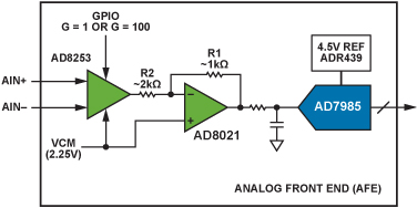
Since the complete system’s noise budget is 15 nV/√Hz max, referred to the input (RTI), it is useful to calculate the dominant noise sources of each block to ensure that the 15‑nV/√Hz hard limit is not exceeded. The AD8021 has an input-referred noise spec of <3 nV/√Hz, which is negligible when referred back to the input of the gain-of-100 AD8253 stage. The AD7985 has a specified SNR of 89 dB, using an external 4.5-V reference, for a noise resolution of <45 μV rms. Considering the Nyquist bandwidth of 300 kHz for the ADC, it will contribute ~83 nV/√Hz across this bandwidth. When referred back to the input of the AD7985, its <1 nV/√Hz will be negligible in the system, where the RTI noise sources are summed using a root-sum-of-squares calculation.
A further benefit of using the AD8253 is that it has digital gain control, which allows the system gain to be dynamically changed in response to changes in the input. This is achieved intelligently using the system’s digital signal processing capability.
The main function of digital processing in this application is to produce a higher-resolution output, using the AD7985 16-bit conversion results. This is achieved by decimating the data and switching the analog input gain automatically, depending on the input amplitude. This oversampling results in a lower output data rate than ADC sample rate, but with a greatly increased dynamic range.
To prototype the digital side of this application, a field-programmable gate array (FPGA) was used as the digital core. To rapidly debug the system, the analog circuitry and the FPGA were consolidated into a single board, shown in Figure 5, using the system demonstration platform (SDP) connector standard to allow easy USB connectivity to the PC. The SDP is a combination of reusable hardware and software that allows easy control of and capture from hardware over the most commonly used component interfaces.

The basic control flow is as follows:
- After power-up, a zero calibration operation is performed. The differential analog inputs of the AD8253 are shorted to ground and an AD7985 conversion is performed at each gain setting. The ADC values are stored for later use.
- After calibration, the AD7985 is given a periodic conversion start signal at a preset rate by the FPGA, in this case, approximately 600 kSPS. Each ADC result is read into the FPGA and passed to both the decimation and gain blocks.
- The gain block looks at the current ADC result, the previous ADC result, and the current gain setting—and determines what the most appropriate gain setting would be for the next ADC conversion. This process is detailed below.
- The decimation block takes in each ADC sample, the current PGA gain setting for that sample, and the calibration values that were stored earlier in the process. After 72 ADC samples have been received, the 23-bit output result is the average value of the 72 samples, with offset and gain taken into account.
- This 23-bit result is then converted into a twos-complement code and received from the FPGA in a format compatible with the Blackfin serial port (SPORT) and captured by the SDP-B hardware. The process is then repeated with a new word after every 72 ADC samples.
The two key modules implemented in the FPGA are the decimator and gain calculator. Detailed descriptions of each block follow.
Decimator
This block has an internal state machine that manages some sequential data-processing steps:
Each individual AD7985 sample is normalized to the same scale. For example: 4 mV input to the AD7985, with a 4.5-V reference, gives a code (4 mV/4.5 V × 65535) = 58 with G = 1. With G = 100, the ADC sees 400 mV at the input and gives an output code of 5825. For an ADC sample taken with an analog front-end (AFE) gain of 1, the sample must be multiplied by 100 to counteract the scaling effect when the AFE has a gain of 100. This ensures that these samples can be averaged and decimated correctly, regardless of the AFE gain setting.
With the decimator function in place, an initial test can be performed on the analog inputs.
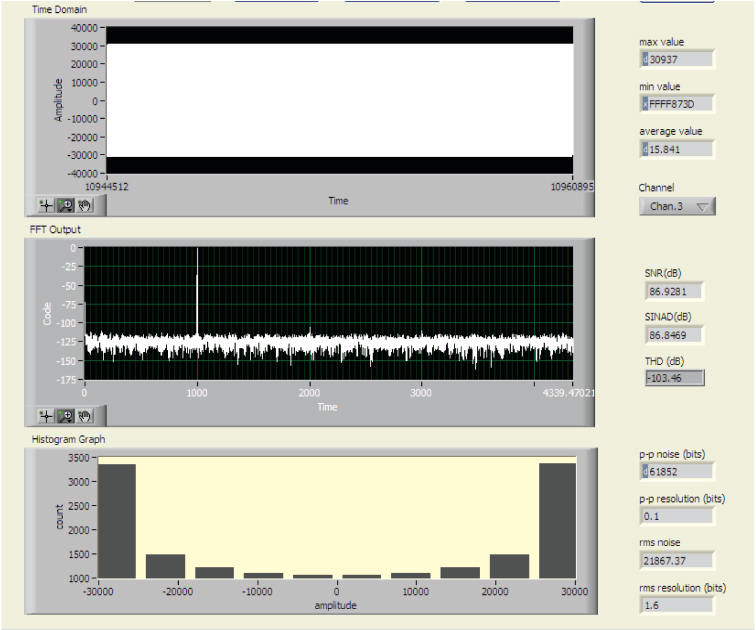
With the inputs shorted, the system can be tested in a high-gain dc mode (see Figure 6).
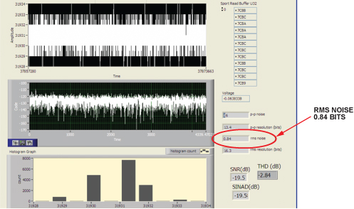
Results show a p-p noise of 6 bits and an excellent rms noise of 0.84 LSB @ 16 bits = 0.654 µV rms. With a 2.12 V rms full-scale range, the dynamic range can be calculated as
DR = 20 log10(FS/rms noise) = ~130 dB
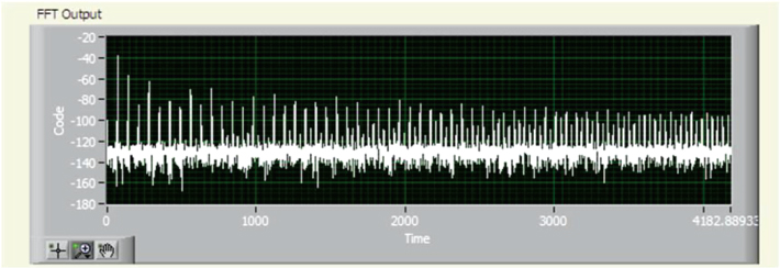
Thus, the system easily meets the dynamic range target regarding noise. When tested with a 50 mV p-p ac analog input, significant distortion was noticed in the frequency domain (see Figure 7). This particular input amplitude highlights the worst case for the system—when the ac input amplitude is slightly larger than the range that is handled by the Gain = 100 mode and the system is regularly switching between the two modes. This range switching effect can also be exacerbated by the choice of gain thresholds, as discussed below. Mismatch between the offsets in each gain mode will show up as gross harmonic distortion, as the calculated output code jumps by the differential between the offsets in each range.
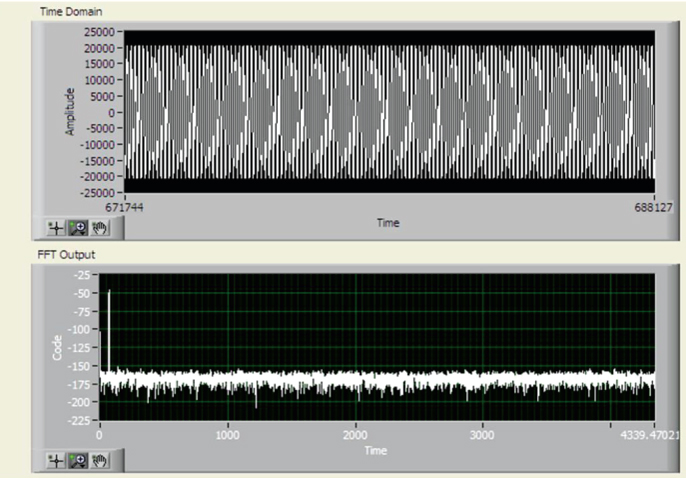
Simply calibrating out the zero offsets at each of the gain ranges can produce a dramatic reduction of signal distortion. In fact, calibration alone can reduce the harmonics by approximately 50 dB, as shown in Figure 8. With even a worst-case input tone, the harmonics have been reduced to the –110 dB FS level.

The calibrated offset is removed from the normalized sample. Since calibration is performed at both gain settings, the offset removed depends on the gain at the time the ADC sample was taken.
The normalized and offset-corrected sample is added into an accumulator register, which is reset at power-up and each time 72 samples have been received. When 72 samples have been received and added to the accumulator, the sum is passed to the divider, which divides the value in the accumulator by 72 to produce a 23-bit averaged result. An output flag is set to indicate that the division is complete and a new result is ready.
Gain Setting
This module outputs a new gain setting based on the current gain setting, two raw ADC samples, and some hard-coded threshold figures. Four thresholds are used in the system; selection of these thresholds is critical to maximizing the analog input range of the system, ensuring the G = 100 mode is used for as much of the signal range as possible, while also preventing the ADC input from being overranged. Note that this gain block operates on every raw ADC result, not on data that has been normalized. Bearing this in mind, an illustrative example of some thresholds that could be used in a system such as this (assuming a bipolar system with a midscale of zero) is as follows:
T1 (positive lower threshold): +162 (162 codes above midscale)
T2 (negative lower threshold): –162 (162 codes below midscale)
T3 (positive upper threshold): +32,507 (260 codes below positive full-scale)
T4 (negative upper threshold): –32,508 (260 codes above negative full-scale)
When in G = 1 mode, the inner limits, T1 and T2, are used. When an actual ADC result is between T1 and T2, gain is switched to G = 100 mode. This ensures that the analog input voltage that the ADC receives is maximized as quickly as possible.
When in G = 100 mode, the outer limits, T3 and T4, are used. If an ADC result is predicted to be above T3 or below T4, the gain is switched to the G = 1 mode to prevent the input of the ADC from being overranged (see Figure 9).
When in G = 100 mode, if the algorithm predicts that the next ADC sample would be just outside the outer threshold (using a very rudimentary linear prediction), giving an ADC result of +32,510, the gain is switched to G = 1, and instead of +32,510 the next ADC result is +325.
In a system like this, to prevent chatter (rapidly repeated gain-switching around the threshold value), hysteresis (separation of the 100 to 1 and 1 to 100 switching levels) is important in determining the correct threshold limits. In the calculations of the actual limits used in this example, significant hysteresis is built in. If the system switches from the high-gain (G = 100) mode to the low-gain (G = 1) mode, the system’s analog input voltage would have to be reduced by almost 50% in order to revert to the high-gain mode.
Performance of Full System
With fully optimized gain and decimation algorithms, the full system is ready to be tested. Figure 10 shows the system response to a large-signal input tone of –0.5 dBFS running at 1 kHz. When the PGA gain of 100 is factored in, the dynamic range achieved is 127 dB.
Similarly, when tested for small-signal inputs in Figure 11, with an input tone of 70 Hz at –46.5 dBFS, up to 129 dB of dynamic range is achieved. The improvement in performance at the smaller input tone is expected, as no active switching of gain ranges occurs during this measurement.
Conclusion
The system’s performance relies on the ability to switch the gain dynamically to handle both small- and large-signal inputs. While ∑-∆ technology provides excellent dynamic range, the SAR-based solution offers a way to dynamically change the front-end gain based on the input signal, without compromising system performance. This allows both small-signal and large-signal ac and dc inputs to be measured in real-time without waiting for system settling time or incurring large glitches due to delayed gain changing.
The key to the system is the ADC oversampling technique combined with the predictive gain-setting algorithm. Critical to the gain algorithm is how the input signal’s slew rate is handled. For higher input slew rates, it could be necessary to customize the gain setting to respond more quickly to a signal that is approaching a level where the ADC input could be overranged. This could be achieved by tightening the thresholds used or with a more complex predictive analysis of the input signal using multiple samples instead of just two as described in this example. Conversely, in a system with a very low input slew rate, the thresholds could be widened to make greater use of the high gain mode without over-ranging the ADC input.
Although this article features the AD7985 ADC, the techniques used are applicable to other high-speed converters from Analog Devices. Using a faster ADC sampling rate, the end user could trade increased input bandwidth and faster output data rate for an increased oversampling ratio, achieving even greater dynamic range.
By utilizing additional gain ranges of the AD8253 VGA, instead of just G = 1 and G = 100, the impact of the gain change could be further minimized. In the current example, a small amount of distortion is introduced when the gain is switched. However, if the G = 10 range were to be used, for a three-step gain with an additional calibration point, a better system THD specification could be achieved.

