Digital potentiometers (digiPOTs) provide a convenient way to adjust the ac or dc voltage or current output of sensors, power supplies, or other devices that require some type of calibration—with timing, frequency, contrast, brightness, gain, and offset adjustment being just a few of the possibilities. Digital setting avoids virtually all of the problems associated with mechanical potentiometers, such as physical size, mechanical wear out, wiper contamination, resistance drift, and sensitivity to vibration, temperature, and humidity—and eliminates layout inflexibility resulting from the need for screwdriver access.
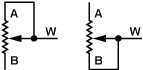
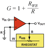
The digiPOT can be used in two different modes: potentiometer or rheostat. In potentiometer mode, shown in Figure 1, three terminals are available; the signal is connected across Terminals A and B, while Terminal W (as in wiper) provides the attenuated output voltage. When the digital ratio-control input is all zeros, the wiper is typically connected to Terminal B.

When the wiper is hardwired to either end, the potentiometer becomes a simple variable resistor, or rheostat, as shown in Figure 2. The rheostat mode permits a smaller form factor, since fewer external pins are required. Some digiPOTs are available only as rheostats.
There are no restrictions on the polarity of currents or voltages appearing at the digiPOT resistance terminals, but the amplitude of ac signals cannot exceed the power-supply rails (VDD and VSS)—and the maximum current, or current density, should be limited when the part is operated in rheostat mode, especially at lower resistance settings.
Typical Applications
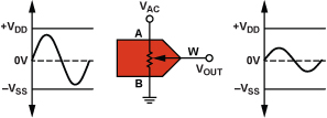
Signal attenuation is inherent in potentiometer mode, for the device is basically a voltage divider. The output signal is defined as: VOUT = VIN × (RDAC/RPOT), where RPOT is the nominal end-to-end resistance of the digiPOT, and RDAC is the digitally selected resistance between W and the reference pin of the input signal, typically Terminal B, as shown in Figure 3.
Signal amplification requires an active component, typically an inverting or noninverting amplifier. Either potentiometer or rheostat mode can be used, with the appropriate gain equation.
Figure 4 shows a noninverting amplifier using the device as a potentiometer to adjust the gain via feedback. Since the fraction of output fed back, RAW/(RWB + RAW), must be equal to the input, the idealized gain is
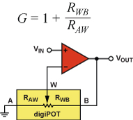
The gain of this circuit, inversely proportional to RAW, increases rapidly as RAW approaches zero, defining a hyperbolic transfer function. To limit the maximum gain, insert a resistor in series with RAW (and in the denominator of the gain equation).
If a linear gain relationship is desired, the rheostat mode can be used in conjunction with a fixed external resistor, as shown in Figure 5; the gain is now defined as:
For best performance, connect the lower capacitance terminal (the W pin in newer devices) to the op-amp input.
Advantages of digiPOTs for Signal Amplification
The circuits shown in Figure 4 and Figure 5 have high input impedance and low output impedance, and can work with unipolar and bipolar signals. digiPOTs can be used in vernier operation to provide greater resolution over a reduced range with fixed external resistors, and can be used in op-amp circuits with or without signal inversion. In addition, they have low temperature coefficients—typically 5 ppm/°C in potentiometer mode and 35 ppm/°C in rheostat mode.
Limitations of digiPOTs for Signal Amplification
When handling an ac signal, digiPOT performance is limited by bandwidth and distortion. Bandwidth is the maximum frequency that can pass through the digiPOT with less than 3-dB attenuation due to parasitic components. Total harmonic distortion (THD)—here defined as the ratio of the rms sum of the next four harmonics to the fundamental value of the output—is a measure of signal degradation as it passes through the device. The performance limits implied by these specifications are caused by the internal digiPOT architecture. An analysis will be helpful in order to fully understand these specifications and reduce their negative effects.
The internal architecture has evolved from the classical serial resistor array, shown in Figure 6a, to the segmented architecture, shown in 6b. The main improvement is the decreased number of internal switches required. In the first case, a serial topology, the number of switches is N = 2n, where n is the resolution in bits. With n = 10, 1024 switches are required.
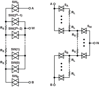
The proprietary (patented) segmented architecture uses a cascade connection that minimizes the total number of switches. The example of Figure 6b shows a two-segment architecture, formed by two types of blocks: MSB on the left, and LSB on the right.
The upper and lower blocks at left are strings of switches for the coarse bits (MSB segment). The block at right is a string of switches for the fine bits (LSB segment). The MSB switches establish a coarse approximation to the RA/RB ratio. Because the total resistance of the LSB string is equal to a single resistive element in the MSB strings, the LSB switches establish the fine portion of the ratio at any point of the main string. The A and B MSB switches are complementary coded.
The number of switches in the segmented architecture is:
N = 2m + 1 + 2n – m,
where n is the total number of bits and m the number of bits of resolution in the MSB word. For example, if n = 10 and m = 5, 96 switches are required.
The segmented scheme requires fewer switches than the conventional string:
Difference = 2n – (2m + 1 + 2n – m)
In this example, the savings would be
1024 – 96 = 928!
In both architectures, switches are responsible for choosing among the different resistance values, making it important to understand the ac error sources in an analog switch. These CMOS (complementary-metal-oxide semiconductor) switches are made up of P-channel and N-channel MOSFETs in parallel. This basic bilateral switch maintains a fairly constant resistance (RON) for signals up to the full supply rails.
Bandwidth
Figure 7 shows the parasitic components that affect the ac performance of CMOS switches.
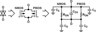
CDS = drain-source capacitance; CD = drain-gate + drain-bulk capacitance; CS = source-gate + source-bulk capacitance.
The transfer relationship is defined in the equation below, where these assumptions have been applied:
- Source impedance is 0 Ω
- No external load contribution
- No contribution from CDS
- RLSB << RMSB

where:
RDAC is the resistance setting
RPOT is the end-to-end resistance
CDLSB is the total drain-gate + drain-bulk capacitance in the LSB segment
CSLSB is the total source-gate + source-bulk capacitance in the LSB segment
CDMSB is the drain-gate + drain-bulk capacitance in the MSB switch
CSMSB is the source-gate + source-bulk capacitance in the MSB switch
moff is the number of off switches in the signal MSB path
mon is the number of on switches in the signal MSB path
The transfer equation has many factors and is somewhat code-dependent, so the following further assumptions are used to simplify the equation
CDMSB + CSMSB = CDSMSB
CDLSB + CSLSB >> CDSMSB
(CDLSB + CSLSB) = CW (specified in the data sheet)
The CDS contribution adds a zero in the transfer equation, but since this occurs typically at much higher frequency than the pole, an RC low-pass filter is the dominant response. A good approximation of the simplified equation is:
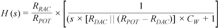
and the bandwidth (BW) is defined as:
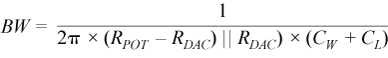
where CL is the load capacitance.
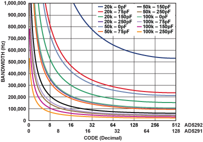
The BW is code dependent, and the worst case is when the code is at half scale, a digital value of 29 = 512 for the AD5292 and 27 = 128 for the AD5291 (see Appendix). Figure 8 shows the low-pass filtering effect as a function of code for various nominal resistance and load capacitance values.
The parasitic track capacitance of the PC board should be taken into account, otherwise the maximum BW will be lower than expected; the track capacitance can be calculated straightforwardly as

where
εR is the dielectric constant of the board material
A is the track area (cm2)
d is the distance between layers (cm)
For example, assuming FR4 board material with two signal layers and power/ground planes, εR = 4, track length = 3 cm, width = 1.2 mm, and distance between layers = 0.3 mm; the total track capacitance is about 4 pF.
Distortion
The THD is used to quantify the nonlinearity of the device as an attenuator. This nonlinearity is due to the internal switches and their RON variation with voltage. An exaggerated example of amplitude distortion is shown in Figure 9.

The RON of a switch is quite small when compared with the resistance of a single internal passive resistor, and its variation over the signal range is even smaller. Figure 10 shows a typical on-resistance characteristic.

The resistance curve does depend on the supply voltage rails; the internal switches have the lowest RON variation at maximum supply voltage. If the supply voltage is decreased, the RON variation, and hence the nonlinearity, increases. Figure 11 compares RON variation at two supply levels for a low-voltage digiPOT.

The THD depends on multiple factors and is thus hard to quantify, but assuming a 10% variation in RON, the following equation can be used as a rough approximation:

As a general rule, the higher the nominal digiPOT resistance (RPOT), the better the THD, as the denominator is larger.
Trade-Offs
Distortion and bandwidth both decrease with increased RPOT, so it is not possible to improve one specification without penalizing the other. So the circuit designer must choose an appropriate balance. This is also true at the device design level, since the IC designer must balance the parameters in the design equations:

where
COX is the oxide capacitance
μ is the mobility constant of the electron (NMOS) or hole (PMOS)
W is the width
L is the length
Biasing
From the practical point of view one must make the best of these specifications. When the digiPOT is used to attenuate an ac signal with capacitive coupling, the lowest distortion is achieved if the signal is biased to the mid-value of the power supply. This means that the switches are working on the most linear portion of the resistance characteristic.
One approach is to use a dual supply and simply ground the potentiometer to the power-supply common. The signal can then have a positive-negative swing. Another way, if a single supply is required, or the particular digiPOT doesn’t support dual supply, is to add an offset voltage of VDD/2 to the ac signal. This offset voltage must be added at both resistor terminals, as shown in Figure 12.

If a signal amplifier is required, an inverting amplifier, with a dual supply, as shown in Figure 13, is preferred over the noninverting amplifier for two reasons:
- Provides better THD performance because the virtual ground at the inverting pin will center the switch resistance in the middle of the voltage range.
- As the inverting pin is at virtual ground, the wiper capacitance, CDLSB, is almost canceled to obtain a small increase in bandwidth (but one must pay attention to circuit stability).

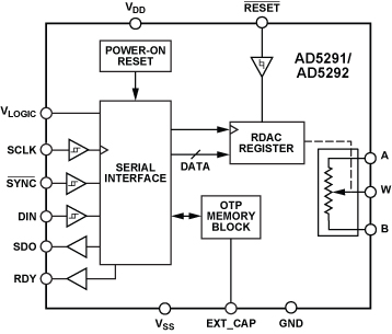
APPENDIX—ABOUT THE AD5291/AD5292
256-/1024-Position Digital Potentiometers Are 1% Accurate, 20-Time Programmable
The AD5291/AD5292 digital potentiometers, shown in Figure 14, feature 256-/1024-position resolution. End-to-end resistance options of 20 kΩ, 50 kΩ, and 100 kΩ are available, with better than 1% tolerance—and temperature coefficients of 35 ppm/°C in rheostat mode and 5 ppm/°C (ratio) in divider mode. The devices perform the same electronic adjustment function as mechanical potentiometers, but are smaller and more reliable. Their wiper position can be adjusted via an SPI-compatible interface. Unlimited adjustments can be made before blowing a fuse to fix the wiper position, a process analogous to putting epoxy on a mechanical trimmer. This process can be repeated up to 20 times (“removing the epoxy”). Operating on a single 9-V to 33-V supply or dual ±9-V to ±16.5-V supplies, the AD5291/AD5292 dissipate 8 μW. Available in 14-lead TSSOP packages, they are specified from –40°C to +105°C.