Introduction
In traditional transceiver designs, 50-Ω single-ended interfaces are widely used in RF and IF circuits. When circuits are interconnected, they should all see matching 50-Ω output and input impedances. In modern transceiver designs, however, differential interfaces are frequently used to obtain better performance in IF circuits, but implementing them requires designers to confront several common issues, including impedance matching, common-mode voltage matching, and difficult gain calculations. An understanding of differential circuits in transmitters and receivers is helpful for optimizing gain matching and system performance.
Differential Interface Advantage
Differential interfacing has three main advantages. First, differential interfacing can suppress external interference and ground noise. Second, even-order output distortion components can be suppressed. This is very important with zero-intermediate-frequency (ZIF) receivers because even-order components appearing in the low-frequency signal cannot be filtered out. Third, the output voltage can be twice that of single-ended output, thus improving output linearity by 6 dB on a given power supply.
This article discusses interfacing solutions for three cases: a ZIF receiver, a superheterodyne receiver, and a transmitter. These three architectures are widely used in wireless remote radio units (RRU), digital repeaters, and other wireless instruments.
ZIF Receiver Interface Design and Gain Calculation
In zero-IF (ZIF) receiver designs, the IF signal is complex, with dc and very low frequency signals providing useful information. Typical demodulators may provide optimum performance when driving 200-Ω to 450-Ω loads, and ADC drivers generally have input impedance other than 50-Ω, so interfacing systems with dc-coupled circuits is both critical and difficult.
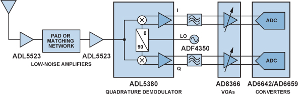
Figure 1 shows a ZIF receiver configuration using two ADL5523 low-noise amplifiers (LNAs), an ADL5380 400-MHz to 6000-MHz quadrature I/Q demodulator, an ADF4350 wideband synthesizer as a local oscillator (LO), and an AD8366 two-channel digitally programmable variable-gain amplifier (VGA). Table 1 shows the relevant ADL5380 interface and gain parameters.
| Test Condition |
VS = 5 V, TA = 25°C, fLO = 900 MHz, fIF = 4.5 MHz, PLO = 0 dBm, ZIN = 50 Ω |
|
| Parameters |
Values |
Comments |
| VoltageConversion Gain |
6.9 dB |
450-Ω differential load on I and Q outputs |
| 5.9 dB |
200-Ω differential load on I and Q outputs |
|
| Common-Mode Output Voltage |
2.5 V |
ADJ connected to VS |
| I/Q Differential Output Impedance |
50 Ω |
|
When interfaced with the AD8366, which has a 217-Ω differential input impedance, the ADL5380 has 5.9-dB voltage gain and –0.5-dB power gain [5.9 dB – 10log (217/50)]. For best performance, the common-mode voltage between the ADL5380 and AD8366 is set to 2.5 V by connecting the ADL5380 ADJ pin to VS. A differential fourth-order Butterworth low-pass filter with 0.5-dB insertion loss, placed between the ADL5380 and the AD8366, suppresses noise and unwanted high-frequency components. While the filter will cause some mismatch, it will be tolerable at baseband frequencies.
Table 2. AD8366 Interface and Gain Parameters| Test Condition |
VS = 5 V, TA = 25°C, ZS = 200 Ω, ZL = 200 Ω, f = 10 MHz |
|
| Parameters |
Values |
Comments |
| VoltageConversion Gain |
4.5 dB |
Minimum digital gain setting |
| 20.25 dB |
Maximum digital gain setting |
|
| Common-Mode Output Voltage |
1.5 V |
Minimum |
| 2.5 V |
Maximum or input self-bias |
|
| Differential Input Impedance |
217 Ω |
|
| Common-Mode Ouput Voltage |
1.6 V |
Minimum |
| 3 V |
Maximum |
|
| 2.5 V | VCMA and VCMB left floating | |
| Differential Output Impedance |
28 Ω |
|
| Linear Output Swing |
6 V p-p |
1-dB gain compression |
The common-mode output voltage of the AD8366 can be set to 2.5 V; it has best linearity when VCM is left floating. Unfortunately, the AD6642 has best performance with 0.9-V common-mode input voltage (0.5 × AVDD). Because the common-mode output voltage of the AD8366 must be between 1.6 V and 3 V, the AD6642 VCM and AD8366 VCM terminals cannot be connected directly, and resistors must be used to divide the AD8366 common-mode output voltage down to 0.9 V.
For best performance, the AD8366 should drive a 200-Ω load. To achieve the desired common-mode level and impedance match, 63-Ω series resistors and 39-Ω shunt resistors are added after the AD8366. This resistor network will attenuate power gain by 4 dB.
The AD8366 output can swing 6 V p-p, but the 4-dB attenuation provided by the resistor network limits the voltage seen by the AD6642 to 2.3 V p-p, protecting it from damage caused by big interference spikes or uncontrolled gains.
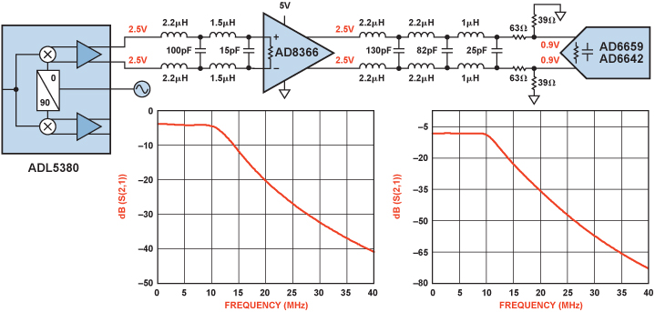
A differential sixth-order Butterworth low-pass filter with 1.5-dB insertion loss, placed between the AD8366 and the AD6642, filters unwanted high-frequency components. The complete differential interface for the I channel is shown in Figure 2.
To preserve enough margin to account for gain variation over temperature, the AD8366 gain is set to 16 dB for the normal mode.
In this configuration, the gain of the whole signal chain is
5.9 dB – 10log (217/50) – 0.5 dB + 16 dB – 10log (200/217) – 1.5 dB – 4 dB
= 9.9 dB.
The two LNAs inserted in cascade ahead of the ADL5380 achieve 32 dB of gain. With the analog-to-digital converter configured for a 2-V p-p swing and 78-Ω equivalent input impedance, it is able to handle a –34-dBm single-tone RF input signal. If the input signal has a 10-dB peak-to-average ratio (PAR) when modulated, a –41-dBm input signal is the maximum signal that the receiver can handle without changing the VGA setting.
In the other words, voltage gain can be used to calculate the signal chain link budget. When the input port impedance is equal to that of the output port, the voltage gain is equal to power gain. The voltage gain of the whole signal chain is
32 dB + 5.9 dB – 0.5 dB + 16 dB – 1.5 dB – 8 dB = 43.9 dB.
For single-tone signal input, to get a 2-V p-p swing range, the proper input power is
8 dBm – 43.9 dB + 10log (78/50) = –34 dBm.
The result is a close match to the calculated power gain.
In some applications, the ADL5380 may need to be connected directly to the AD6642, in which case a 500-Ω resistor can be added to the AD6642 differential inputs to improve matching. The ADL5380 voltage gain will be 6.9 dB, with the same common-mode problem as with the AD8366. A 160-Ω series resistor and 100-Ω shunt should be used to achieve a 500-Ω load and the desired common-mode voltage. Again, the resistor network attenuates the voltage by 8 dB (and the power by 4 dB).
A low-pass filter with 1.5-dB insertion loss, placed between the ADL5380 and AD6642, filters unwanted frequency components. The input impedance is 50 Ω, and the output impedance is 500 Ω. In this configuration, the gain of the whole signal chain is
6.9 dB – 10log (500/50) – 1.5 dB – 4 dB = –8.6 dB.
Superheterodyne Receiver Interface Design and Gain Calculation
In superheterodyne receivers, the system uses ac coupling, so the dc common-mode voltage does not have to be considered when interfacing these circuits.
Many mixers, such as the ADL535x and ADL580x, have 200-Ω differential output impedance, so the power gain and voltage gain are presented separately for different output impedances.
Figure 3 shows one channel of a superheterodyne receiver implemented with an ADL5523 low-noise amplifier; an ADL5356 dual balanced mixer with LO buffer, IF amplifier, and RF balun; a low-pass filter; an AD8376 dual ultralow distortion IF VGA; another low-pass filter; and an AD6642 dual IF receiver.
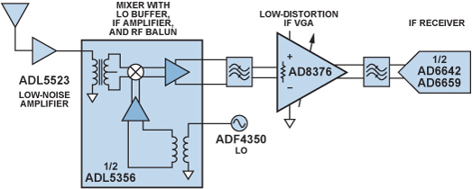
This design uses a 140-MHz IF and 20-MHz bandwidth, so the parts can be ac-coupled.
The AD5356 has best performance with a 200-Ω load, but the AD8376 has 150-Ω input impedance. Thus, to suppress mixer output spurs and provide better impedance matching, the differential LC filter must have 200-Ω input impedance and 150-Ω output impedance. In applications where the output band signal must be suppressed by a sharp filter, a differential SAW filter can be used, but this introduces loss and group delay in the receiver signal chain. A differential fourth-order band-pass Butterworth filter may be suitable for many wireless receivers because the RF filter can provide enough attenuation for out-of-band interference.
Table 3. ADL5356 and AD8376 Interface and Gain Parameters| ADL5356 Test Condition |
VS = 5 V, TA = 25°C, fRF = 1900 MHz, fLO = 1760 MHz, LO power = 0 dBm |
|
| Parameters |
Values |
Comments |
| VoltageConversion Gain |
14.5 dB |
ZSOURCE = 50 Ω, differential ZLOAD = 200 Ω differential |
| Common-Mode Output Voltage |
2.5 V |
ADJ connected to VS |
| Power Conversion Gain |
8.2 dB |
Including 4:1 IF port transformer and PCB loss |
| AD8376 Test Condition |
VS = 5 V, TA = 25°C, RS = RL = 150 Ω at 140 MHz |
|
| Parameters |
Values |
Comments |
| Differential Input Resistance |
150 Ω |
|
| Voltage Conversion Gain |
–4 dB |
Minimum digital setting |
| 20 dB | Maximum digital setting |
|
| Output Impedance |
16 kΩ || 0.8 pF |
|
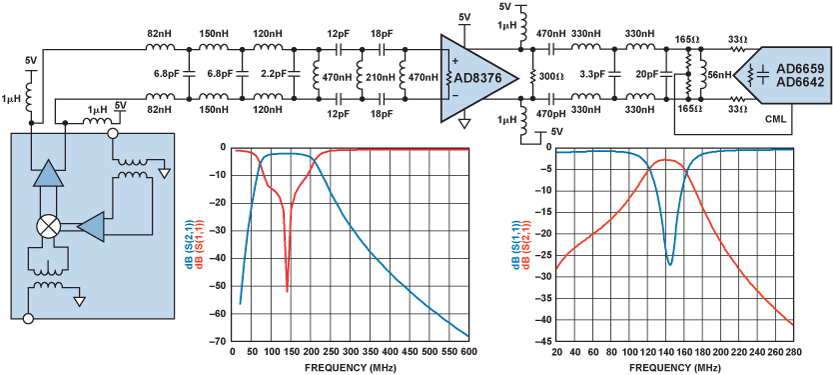
The AD8376’s current-output circuit has high output impedance, so 150-Ω is needed between its differential outputs. Another differential filter must attenuate the second- and third-harmonic distortion components, so this 150-Ω load is divided into two parts. First, a 300-Ω resistor is installed in the output of the AD8376. Another 300-Ω resistor is formed by two 165-Ω resistors and the ADC’s 3-kΩ input impedance. The two 165-Ω resistors also provide the dc common-mode voltage for the ADC input. The LC filter’s input and output impedances are both 300 Ω. Perfect source and load matching is very important for high-IF applications. The complete interface is shown in Figure 4.
In the receiver, a 20-dB LNA is installed ahead of the mixer. The filter after the mixer has 2-dB insertion loss; the filter between the AD8376 and the ADC has 1.2-dB insertion loss. The AD8376 gain is set to 14 dB to provide enough margin to account for temperature variation. The overall gain of the receiver is
20 dB + 8.2 dB – 2 dB + 14 dB – 1.2 dB = 39 dB.
To limit the ADC input voltage to less than 2 V p-p, the power transmitted to the 150-Ω resistance (300 Ω || (165 Ω × 2) || 3 k Ω) should be smaller than 5.2 dBm. The maximum input power for the receiver is thus –33.8 dBm for a single-tone signal. If the input signal is a 10-dB PAR modulation signal, the maximum input signal using this gain setting is –40.8 dBm.
Transmitter Interface Design and Gain Calculation
For Tx-channel designs, both ZIF and superheterodyne architectures have similar interface characteristics, and both need dc coupling between the TxDAC® and the modulator. Most modulators’ IF input circuits should be biased by a dc voltage externally; the TxDAC output can provide dc bias for the modulator in a dc-coupled mode. Most high-speed DACs have current outputs, so an output resistor is needed to produce an output voltage for the modulator.
Figure 5 shows a superheterodyne or ZIF transmitter implemented with an AD9122 TxDAC, a low-pass filter, an ADL537x quadrature modulator, another RF filter, an ADF4350 synthesizer, an ADL5243 digitally controlled VGA, a power amplifier, and an AD562x DAC to control the power amplifier’s (PA) gate voltage.
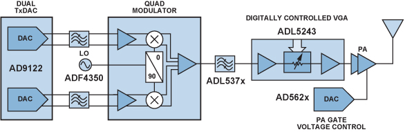
For the AD9122, the full-scale output current can be set between 8.66 mA and 31.66 mA. For full-scale currents greater than 20 mA, the spurious-free dynamic range (SFDR) is decreased, but the output power and ACPR of the DAC decrease with lower full-scale current settings. A suitable compromise is a 0-mA to 20-mA current output consisting of a 20-mA ac current riding on a 10-mA dc level.
Table 4. AD9122 and ADL5372 Interface and Gain Parameters| AD9122 Test Condition |
AVDD33 = 3.3 V, DVDD33 = 3.3 V, DVDD18 = 1.8 V, CVDD18 = 1.8 V |
|
| Parameters |
Values |
Comments |
| Full-Scale Output Current |
8.66 mA |
Minimum digital full scale setting |
| 31.66 mA | Maximum digital full scale setting | |
| Output Resistance |
10 MΩ |
|
| ADL5372 Test Condition |
VS = 5 V, TA = 25°C, fLO = 1900 MHz, fIF = 140 MHz |
|
| Parameters |
Values |
Comments |
| Output Power |
7.1 dBm |
VIQ = 1.4 V p-p differential |
| I and Q Input Bias Level |
0.5 V |
Recommended |
| Differential Input Impedance |
2900 kΩ |
|
The input circuit of the ADL5372 needs a 0.5-V common-mode voltage, which is provided by a 10-mA dc current flowing through a 50-Ω resistor. The 0-mA to 20-mA ac current is shared by two 50-Ω resistors and a 100-Ω resistor. The ac voltage between the modulator inputs is thus 20 mA × ((50 × 2) || 100) = 1 V p-p. The filter between the TxDAC and the modulator removes unwanted frequency components. The input and output impedance of the filter is 100 Ω. The complete interface is shown in Figure 6.
With a 50-Ω output, the voltage conversion gain of the ADL5372 is 0.2 dBm. With a 13-dB PAR modulator signal, the average power must be reduced by at least 15 dB for the Tx digital predistortion process. With a 1-V p-p single-tone input to the ADL5372, the average modulator output power is 7.1 dBm – 2.9 dBm = 4.2 dBm. If the 2.2-dBm insertion loss of the low-pass filter is considered, the peak output power is 4.2 dBm – 2.2 dBm = 2 dBm. In this state, an average output power of –10 dBm is presented at the output of the modulator.
With an 11-dBm average power signal, a PA-driver with 26-dBm P1dB is needed in the Tx signal chain. If a 2-dB insertion-loss RF filter is needed to suppress LO feedthrough and sideband output of the modulator, then the gain block and PA driver have to provide a total of 21-dB gain. The ADL5243 VGA with integrated gain block, digitally controlled attenuator, and PA driver is suggested for this application.
Conclusion
This paper describes ZIF and superheterodyne receiver differential interfaces for the demodulator, IF VGA, mixer, and analog port of the ADC, as well as transmitter differential interfaces between the TxDAC and FMOD, using Analog Devices parts for active portions of the signal chain. Gain calculations and simulation results are presented for the application filters that were designed for these circuits. Additional information can be found in the following references.
References
Circuit Note CN-0018, Interfacing the ADL5372 I/Q Modulator to the AD9779A Dual-Channel, 1 GSPS High-Speed DAC.
Circuit Note CN-0134, Broadband Low Error Vector Magnitude (EVM) Direct Conversion Transmitter.
Calvo, Carlos. “The differential-signal advantage for communications system design.” EE Times.
