In many markets, demand is increasing for efficient noninverting dc-to-dc converters that can operate in either buck or boost mode, decreasing or increasing the input voltage to a desired regulated voltage—with minimal cost and component count. The inverse SEPIC (single-ended primary inductor converter), also known as the zeta converter, has many properties that make it ideal for this function (Figure 1). An analysis of its operation and implementation with the ADP1877 dual-channel synchronous switching controller will reveal its useful properties for this application.

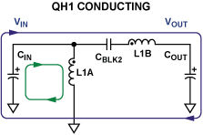
Primary switch QH1 and secondary switch QL1 operate in opposite phase from one another. During the on time, QH1 is conducting and QL1 is off. Current flows in two paths, as shown in Figure 2. The first is from the input, through the primary switch, energy-transfer capacitor (CBLK2), the output inductor (L1B), and the load—finally returning back to the input through ground. The second path is from the input, through the primary switch, the ground-reference inductor (L1A), and back to the input through ground.
During the off time, the switch positions are reversed. QL1 is conducting and QH1 is off. The input capacitor (CIN) is disconnected, but current continues to flow through the inductors in two paths, as shown in Figure 3. The first is from the output inductor, through the load, through ground, and back to the output inductor through the secondary switch. The second path is from the ground-reference inductor, through the energy-transfer capacitor, the secondary switch, and back to the ground-reference inductor.

Applying the principles of inductor volt-second balance and capacitor charge balance, one finds the equilibrium dc conversion ratio specified in Equation 1, where D is the converter's duty cycle (on time fraction of the cycle).
 |
(1) |
This suggests that if the duty cycle is greater than 0.5, a higher voltage will be regulated at the output (boost); if the duty cycle is less than 0.5, the regulated voltage will be lower (buck). Other relevant results of this analysis are that the steady-state voltage across the energy-transfer capacitor (CBLK2) is equal to VOUT in a lossless system; the dc value of the current through the output inductor (L1B) is equal to IOUT; and the dc value of the current through the ground-reference inductor (L1A) is IOUT × VOUT/VIN. The energy-transfer capacitor also provides dc blocking from VIN to VOUT. This property can be attractive when there is a risk of a shorted output.
The analysis also shows that the output current in the inverse SEPIC is continuous, yielding a lower peak-to-peak output voltage ripple for a given output capacitor impedance. This allows the use of smaller, less costly output capacitors as compared to the capacitors needed to meet the same ripple requirement with discontinuous output current topologies.
Typically the secondary switch (QL1) is a unidirectional power diode, which limits the peak efficiency of this topology. However, with a single channel of the Analog Devices ADP1877 dual-channel synchronous switching controller (see Appendix), an inverse SEPIC can be designed in a fully synchronous configuration, employing a bidirectional MOSFET as the secondary switch. This allows the peak efficiency to increase considerably, while at the same time decreasing the size and cost of the converter at output currents greater than 1 A.
Figure 4 shows the power stage of the fully synchronous inverse SEPIC configuration, as implemented with the ADP1877 and requiring only three small, inexpensive additional components (CBLK1, DDRV, and RDRV) that dissipate negligible power.

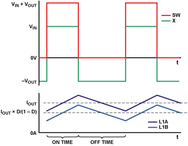
The ideal steady-state waveforms of the inverse SEPIC are shown in Figure 5. The Channel-1 switch node, SW1, (see Figure A in the Appendix) is toggled between VIN + VOUT during the on time and 0 V during the off time. Connecting charge-pump capacitor, CBST, to SW1 imposes a voltage approximately equal to VIN + VOUT + 5 V on the bootstrapped upper rail of the high-side internal driver (BST1 pin) and the output of the high-side driver (DH1 pin) during the on time, thus enhancing the primary floating N-channel MOSFET switch, QH1. Clamping diode, DDRV, ensures that CBLK1 has approximately VOUT + VFWD(DDRV) across it during steady-state output, as referenced from the DH1 pin of the ADP1877 to the gate of QH1. The voltage across CBLK1 keeps the primary switch from developing a gate-to-source voltage that is higher than its threshold during the off time when the X-node voltage is approximately equal to –VOUT.
The ADP1877 has a pulse-skip mode that, when enabled, increases the efficiency at light loads by decreasing the switching rate, delivering just enough energy to the output to keep the output voltage in regulation—considerably decreasing the gate charge and switching loss. This mode can be enabled in both the synchronous inverse SEPIC and synchronous buck topologies. Since only a single channel of the dual-channel ADP1877 is needed for the dc-to-dc conversion circuit of Figure 4, the other channel is available for either topology.
Inductor Coupling and Energy Transfer Capacitor
In Figure 4, power inductors L1A and L1B are shown as coupled. The purpose for coupling the inductors in this topology is to reduce ripple in the output voltage and inductor current, and to increase the maximum potential closed-loop bandwidth—as will be seen in the next section.
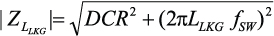
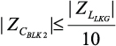
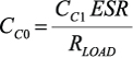
Even though the inductors are coupled, it is undesirable for the coupling to be tight enough to transfer significant energy from one winding to the other through the core. This can be avoided by finding the leakage inductance (LLKG) of the coupled inductor and sizing the energy transfer capacitor (CBLK2) such that the magnitude of its complex impedance is one tenth of the complex series impedance of the leakage inductance and the resistance (DCR) of a single winding, as designated in Equations 2, 3, and 4. Designing the circuit to conform to this relationship minimizes the energy transfer through the coupled core. The leakage inductance can be calculated from the coupling coefficient, commonly found on coupled-inductor data sheets.
 |
(2) | |
 |
(3) | |
 |
(4) |
A 1:1 turns ratio is desirable because it requires half the inductance for each winding that discrete inductors would need for a given level of output voltage ripple.1
Small-Signal Analysis and Loop Compensation
A complete small-signal analysis of the inverse SEPIC converter is beyond the scope of this paper; however, if one follows the following guidelines, the complete analysis becomes academic.
First, many complex impedance interactions at the resonant frequency (fRES) must be calculated initially in order to find the upper limit on the target crossover frequency. When the inductors are uncoupled, this frequency decreases, significantly decreasing the potential maximum closed-loop bandwidth.
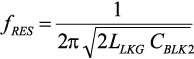 |
(5) |
At this frequency there can be 300° or more of "high-Q" phase lag. To avoid a low phase margin converter across the full load range, one should target a crossover frequency (fUNITY) at one-tenth fRES. Damping this resonance is largely dependent on the output loading resistance and the coupled inductor's dc resistance. To a lesser extent, damping is dependent on the equivalent series resistance (ESR) of the energy-transfer capacitor, and the on resistance of the power MOSFETs (QHl and QL1). Therefore, as the output load resistance varies, one should not be surprised to see the signature of the closed-loop transfer function change dramatically at this frequency.
The coupling coefficient is often not a well controlled parameter, so the target crossover frequency, fUNITY, should be set to a decade below fRES, assuming fRES is less than the switching frequency, fSW. Standard "Type II" compensation—with two poles and a zero—can be used when fUNITY is set appropriately.
 |
(6) |
Figure 6 shows the equivalent circuit of the ADP1877's feedback loop when employed in a synchronous inverse SEPIC buck/boost topology. The upper box contains the power stage and current loop; the lower box contains the voltage feedback loop and compensation circuitry.

The compensation-component values in the lower box can be calculated as follows:
 |
(7) | |
 |
(8) | |
 |
(9) |
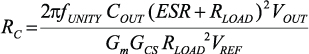
GCS, the transconductance of the converter, is calculated by:
 |
(10) |
COUT is the output capacitance of the converter. ESR is the equivalent series resistance of the output capacitor. RLOAD is the minimum output load resistance. ACS is the current sense gain, which, with the ADP1877, is selectable in discrete steps from 3 V/V to 24 V/V. Gm is the transconductance of the error amplifier, 550 μs for the ADP1877. VREF is the reference voltage that is tied to the positive input of the error amplifier, 0.6 V for the ADP1877.
GCS is a frequency-independent gain term that varies with RDS(ON), the resistance of the secondary switch when enhanced. It is expected that the highest crossover frequency occurs when this resistance and the duty cycle, D, are at their lowest.
To ensure that the compensation clamp voltage is not reached at maximum output current, the highest value of current-sense gain (ACS) that obeys the following inequality should be selected:
 |
(11) |
where ∆IL is the peak-to-peak inductor ripple current.
 |
(12) |
If excessive slope compensation is added, the equations in this section will be less accurate: the dc gain will decrease and the dominant pole location—due to the output filter—will increase in frequency.
Slope Compensation
For synchronous inverse SEPICs implemented with the ADP1877, the subharmonic oscillation phenomenon in current mode controllers2 must be taken into account.
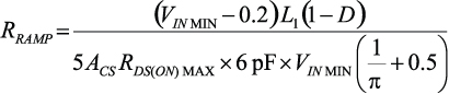
By setting RRAMP according to the following equation, the quality factor of the sampling poles can be set to unity, which prevents subharmonic oscillations,3 assuming fUNITY was set appropriately.
 |
(13) |
It is noteworthy that as RDS(ON)—the resistance of the secondary switch when enhanced—decreases, the Q of the sampling poles also decreases. If this, in conjunction with other related tolerances, results in a Q of less than 0.25, one should perform a simulation to ensure the converter does not have excessive slope compensation and is not "too voltage mode" with tolerance considered. The value of RRAMP must result in a current between 6 μA and 200 μA into the ADP1877's RAMP pin, as calculated with Equation 14.
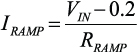 |
(14) |
Power Component Stresses
From the current-flow diagrams in Figure 2 and Figure 3, one can see that the power MOSFETs, when conducting, carry the sum of the inductor currents. Accordingly, the dc component of the current through both switches is
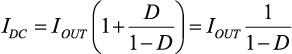 |
(15) |
The ac component of the current through both switches is
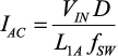 |
(16) |
With these values known, one can quickly calculate the rms values of the current through each switch. In conjunction with the RDS(ON)MAX of the selected MOSFETs, these can be used to ensure that the MOSFETs are thermally stable, with power dissipation low enough to meet the efficiency requirements.
Calculating switching loss in the primary switch accurately is beyond the scope of this paper, but it should be noted that, in transitioning from high-resistance- to low-resistance states, the voltage across the MOSFET will swing from ~VIN + VOUT to ~0 V, and the current through the device will swing from 0 A to IOUT[1/(1 – D)]. Switching loss can be the predominant loss with swings of these magnitudes, a factor one should be aware of when picking a MOSFET for which the reverse transfer capacitance (CRSS) and RDS(ON) are inversely proportional.
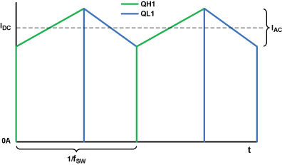
The drain-source breakdown voltage (BVDSS), for both the primary and secondary switches, must be greater than the input voltage plus the output voltage (see Figure 5).
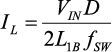
The peak-to-peak output-voltage ripple (∆VRIPPLE) is approximated by
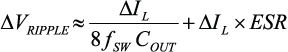 |
(17) |
The rms value of the current through the output capacitor (I rms COUT) is
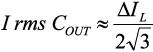 |
(18) |
The peak-to-peak inductor current (∆IL) designated in Equation 12 depends on the input voltage, so one must ensure that, as this parameter varies, the output-voltage ripple does not exceed the specification and the rms current through the output capacitor does not exceed its rating.
For synchronous inverse SEPICs implemented with the ADP1877, the input voltage plus the output voltage must not exceed 14.5 V because the charge-pump capacitor is connected to the switch node, which reaches VIN + VOUT when the primary switch is conducting.
Lab Results
Figure 8 shows the efficiency of the synchronous inverse SEPIC as a function of load current for 5-V output with 3-V and 5.5-V inputs—a common situation for applications that need to toggle between 3.3 V and 5.0 V input rails, or when the input voltage is margined on-the-fly to optimize for system efficiency. With 1-A to 2-A loads, and the input voltage both above and below the output voltage, the efficiency of the converter reaches over 90%.
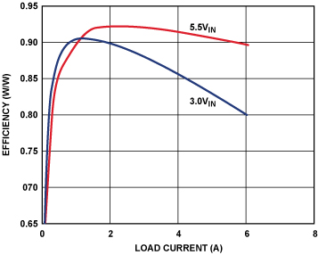
The bill of materials for the relevant power components associated with Figure 8 is seen in Table 1; it includes only common off-the-shelf components. A comparable asynchronous design using an industry-leading Schottky diode with a low forward-voltage drop in place of QL1 is almost 10% less efficient at full load at both input voltages. The asynchronous design would also be larger and more expensive and would be likely to require a costly heat sink.
Table 1. Power Components
| Designator | Part Number | Manufacturer | Value | Package | Comment |
| QH1/QL1 | FDS6572A | Fairchild Semiconductor | 20 BVDSS | SO8 | Power MOSFET/6 mΩ (max) @ 4.5 Vgs @ 25°C Tj |
| L1A/B | PCA20EFD-U10S002 | TDK | 3.4 µH per winding | 30 mm × 22 mm × 12 mm | 1:1:1:1:1:1 coupled inductor/ferrite/35.8 mΩ (max) DCR per winding |
Conclusion
The need for high efficiency noninverting converters that provide both higher and lower voltages than the input (boost and buck) is increasing in many markets. The Analog Devices ADP1877 dual-channel synchronous switching controller allows the high-loss power diode commonly used in the power stage to be replaced by a low-loss MOSFET. This increase in efficiency can reduce cost and circuit footprint—and allow the system to meet stringent energy requirements. Component values for robust compensation can be quickly calculated by following a few guidelines, and high efficiency can be achieved with common off-the-shelf components.
References
Barrow, Jeff. "Reducing Ground Bounce in DC-to-DC Converters—Some Grounding Essentials." Analog Dialogue. 41-2, pp. 2-7. 2007.
1Ćuk, Slobodan and R.D. Middlebrook. "Coupled-Inductor and Other Extensions of a New Optimum Topology Switching DC-DC Converter." Advances in Switched-Mode Power Conversion. Volumes I & II. Irvine, CA: TESLAco. 1983.
2Erickson, Robert and Dragan Maksimović. Fundamentals of Power Electronics. Chapter 12, Section 1. Norwell, MA: Kluwer Academic Publishers. 2001.
3Ridley, Raymond. "A New Small-Signal Model for Current-Mode Control." PhD Dissertation, Virginia Polytechnic Institute and State University. November 1990.
Appendix
The ADP1877, shown in Figure A, is a Flex-Mode™ (proprietary architecture of Analog Devices, Inc.) dual-channel, switching controller with integrated drivers that drive N-channel synchronous power MOSFETs. The two PWM outputs are phase-shifted by 180°, which reduces the input rms current, thus minimizing required input capacitance.

The boost diodes are built into the ADP1877, thus lowering the overall component count and system cost. The ADP1877 can be set to operate in pulse-skip high-efficiency mode under light load, or in PWM continuous conduction mode.
The ADP1877 includes externally adjustable soft start, output overvoltage protection, externally adjustable current limit, power good, and a programmable oscillator frequency that ranges from 200 kHz to 1.5 MHz. The ADP1877 provides an output voltage accuracy of ±0.85% from –40°C to +85°C and ±1.5% from –40°C to +125°C junction temperature. Powered by a 2.75-V to 14.5-V supply, it is available in a 32-lead, 5 mm × 5 mm LFCSP package.
