So far, we have described the physical architecture of the DSP processor, explained how DSP can provide some advantages over traditionally analog circuitry, and examined digital filtering, showing how the programmable nature of DSP lends itself to such algorithms. Now we look at the process of implementing a finite-impulse- response (FIR) filter algorithm (briefly introduced in Part 2, implemented in ADSP-2100 Family assembly code) on a hardware platform, the ADSP-2181 EZ-Kit Lite&tm;. The implementation is expanded to handle data I/O issues.
Using Digital Filters
Many of the architectural features of the DSP, such as the ability to perform zero-overhead loops, and to fetch two data values in a single processor cycle, will be useful in implementing this filter. Reviewing briefly, an FIR filter is an all-zeros filter that is calculated by convolving an input data-point series with filter coefficients. Its governing equation and direct-form representation are shown in Figure 1.

In this structure, each "z–1 " box represents a single increment of history of the input data in z-transform notation. Each of the successively delayed samples is multiplied by the appropriate coefficient value, h(m), and the results, added together, generate a single value representing the output corresponding to the nth input sample. The number of delay elements, or filter taps, and their coefficient values, determine the filter’s performance.
The filter structure suggests the physical elements needed to implement this algorithm by computation using a DSP. For the computation itself, each output sample requires a number of multiply-accumulate operations equal to the length of the filter.
The delay line for input data and the coefficient value list require reserved areas of memory in the DSP for storing data values and coefficients. The DSP’s enhanced Harvard architecture lets programmers store data in Program Memory as well as in Data Memory, and thus perform two simultaneous memory accesses in every cycle from the DSP’s internal SRAM. With Data Memory holding the incoming samples, and Program Memory storing the coefficient values, both a data value and a coefficient value can be fetched in a single cycle for computation.
This DSP architecture favors programs that use circular buffering (discussed briefly in Part 2 and later in this installment). The implication is that address pointers need to be initialized only at the beginning of the program, and the circular buffering mechanism ensures that the pointer does not leave the bounds of its assigned memory buffer—a capability used extensively in the FIR filter code for both input delay line and coefficients. Once the elements of the program have been determined, the next step is to develop the DSP source code to implement the algorithm.
Developing DSP Software
Software development flow for the ADSP-2100 Family consists of the following steps: architecture description, source-code generation, software validation (debugging), and hardware implementation. Figure 2 shows a typical development cycle.
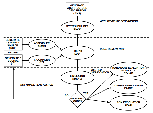
Architecture description: First, the user creates a software description of the hardware system on which the algorithm runs. The system description file includes all available memory in the system and any memory-mapped external peripherals. Below is an example of this process using the ADSP-2181 EZ-Kit Lite.
Source-code generation: Moving from theory into practice, this step—where an algorithmic idea is turned into code that runs on the DSP—is often the most time-consuming step in the process. There are several ways to generate source code. Some programmers prefer to code their algorithms in a high-level language such as C; others prefer to use the processor’s native assembly language. Implementations in C may be faster for the programmer to develop, but compiled DSP code lacks efficiency by not taking full advantage of a processor’s architecture.
Assembly code, by taking full advantage of a processor’s design, yields highly efficient implementations. But the programmer needs to become familiar with the processor’s native assembly language. Most effective is combining C for high-level program-control functions and assembly code for the time-critical, math-intensive portions of the system. In any case, the programmer must be aware of the processor’s system constraints and peripheral specifics. The FIR filter system example in this article uses the native assembly language of the ADSP-2100 Family.
Software validation ("debugging"): This phase tests the results of code generation—using a software tool known as a simulator— to check the logical flow of the program and verify that an algorithm is performing as intended. The simulator is a model of the DSP processor that a) provides visibility into all memory locations and processor registers, b) allows the user to run the DSP code either continuously or one instruction at a time, and c) can simulate external devices feeding data to the processor.
Hardware implementation: Here the code is run on a real DSP, typically in several phases: a) tryout on an evaluation platform such as EZ-Kit Lite; b) in-circuit emulation, and c) production ROM generation. Tryout provides a quick go/no-go determination of the program’s operation; this technique is the implementation method used in this article. In-circuit emulation monitors software debug in the system, where a tool such as an EZ-ICE™ controls processor operation on the target platform. After all debug is complete, a boot ROM of the final code can be generated; it serves as the final production implementation.
Working With the ADSP-2181 EZ-Kit Lite
Our example of the development cycle walks through the process, using the ADSP-2181 EZ-Kit Lite (development package ADDS-21xx- EZLITE) as the target hardware for the filter algorithm. The EZ-Kit Lite, a low-cost demonstration and development platform, consists of a 33-MHz ADSP-2181 processor, an AD1847 stereo audio codec, and a socketed EPROM, which contains monitor code for downloading new algorithms to the DSP through an RS-232 connection (Figure 3).

To complete the architecture description phase, one needs to know the memory and memory-mapped peripherals that the DSP has available to it. Programmers store this information in a system-description file so that the development tools software can produce appropriate code for the target system. The EZ-Kit Lite needs no memory external to the DSP, because available memory on-chip consists of the 16,384 locations of the ADSP-2181’s Program Memory (PM) SRAM, and 16,352 locations of Data Memory (DM) SRAM. (32 DM locations used for system control registers are not available for working code). More information on the ADSP-2181, the EZ-Kit Lite’s architecture, and related topics, can be found in texts mentioned at the end of this article.
Available system resources information is recorded in a system description file for use by the ADSP-2100 Family development tools. A system description file has a .SYS extension. The following list shows a system description file [EZKIT_LT.SYS]:
.system EZ_LITE; /* gives a name to this system */
.adsp2181; /* specifies the processor */
.mmap0; /* specifies that the system boots and that */,
/* PM location 0 is in internal memory */
.seg/PM/RAM/ABS=0/code/data int_pm[16384];
.seg/DM/RAM/ABS=0 int_dm[16352];
.endsys; /* ends the description */
The listing declares 16,384 locations of PM as RAM, starting at address 0, to let both code segments and data values be placed there. Also declared are 16,352 available locations of data memory as RAM, starting at address 0. Because these processors use a Harvard architecture with two distinct memory spaces, PM address 0 is distinct from DM address 0. The ADSP-2181 EZ-Kit Lite’s codec is connected to the DSP using a serial port, which is not declared in the system description file. To make the system description file available to other software tools, the System Builder utility, BLD21, converts the .SYS file into an architecture, or .ACH, file. The output of the System Builder is a file named EZKIT_LT.ACH.
After writing the code, the next step is to generate an executable file, i.e., turn the code into instructions that the DSP can execute. First one assembles the DSP code. This converts the program file into a format that the other development tools can process. Assembling also checks the code for syntax errors. Next, one links the code to generate the DSP executable, using the available memory that is declared in the architecture file. The Linker fits all of the code and data from the source code into the memory space; the output is a DSP executable file, which can be downloaded to the EZ-Kit Lite board.
Generating Filter Code
Part 2 of this series [Analog Dialogue 31-2, page 14, Figure 6] introduced a small assembly code listing for an FIR filter. Here, that code is augmented to incorporate some EZ-Kit Lite-specific features, specifically codec initialization and data I/O. The core filter-algorithm elements (multiply-accumulates, data addressing using circular buffers for both data and coefficients, and reliance on the efficiency of the zero-overhead loop) do not change.
The incoming data will be sampled using the on-board AD1847 codec, which has programmable sampling rate, input gain, output attenuation, input selection, and input mixing. Its programmable nature makes the system flexible, but it also adds a task of programming to initialize it for the DSP system.
Accessing Data
For this example, a series of control words to the codec—to be defined at the beginning of the program in the first section of the listing—will initialize it for an 8-kHz sampling rate, with moderate gain values on each of the input channels. Since the AD1847 is programmable, users would typically reuse interface and initialization code segments, changing only the specific register values for different applications. This example will add the specific filter segment to an existing code segment found in the EZ-Kit Lite software.
This interface code declares two areas in memory to be used for data I/O: "tx_buf", for data to be transmitted out of the codec, and "rx_buf", where incoming data is received. Each of these memory areas, or buffers, contains three elements, a control or status word, left-channel data, and right-channel data. For each sample period, the DSP will receive from the codec a status word, left channel data, and right channel data. On every sample period, the DSP must supply to the codec a transmit control word, left channel data, and right channel data. In this application, the control information sent to the codec will not be altered, so the first word in the transmit data buffer will be left as is. We will assume that the source is a monophonic microphone, using the right channel (no concern about left-channel input data).
Using the I/O shell program found in the EZ-Kit Lite software, we need only be involved with the section of code labeled "input_samples". This section of code is accessed when new data is received from the codec ready to be processed. If only the right channel data is required, we need to read the data located in data memory at location rx_buf + 2, and place it in a data register to be fed into the filter program.
The data arriving from the codec needs to be fed into the filter algorithm via the input delay line, using the circular buffering capability of the ADSP-2181. The length of the input delay line is determined by the number of coefficients used for the filter. Because the data buffer is circular, the oldest data value in the buffer will be wherever the pointer is pointing after the last filter access (Figure 4) . Likewise the coefficients, always accessed in the same order every time through the filter, are placed in a circular buffer in Program Memory.

Algorithm Code
To operate on the received data, the code section published in the last installment can be used with few modifications. To implement this filter, we need to use the multiply/accumulate (MAC) computational unit and the data address-generators.
The ADSP-2181’s MAC stores the result in a 40-bit register (32 bits for the product of 2 16-bit words, and 8 bits to allow the sum to expand without overflowing). This allows intermediate filter values to grow and shrink as necessary without corrupting data. The code segment being used is generic (i.e., can be used for any length filters); so the MAC’s extra output bits allow arbitrary filters with unknown data to be run with little fear of losing data.
To implement the FIR filter, the multiply/accumulate operation is repeated for all taps of the filter on each data point. To do this (and be ready for the next data point), the MAC instruction is written in the form of a loop. The ADSP-21xx’s zero-overhead loop capability allows the MAC instruction to be repeated for a specified number of counts without programming intervention. A counter is set to the number of taps minus one, and the loop mechanism automatically decrements the counter for each loop operation. Setting the loop counter to "taps–1" ensures that the data pointers end up in the correct location after execution is finished and allows the final MAC operation to include rounding. As the AD1847 is a 16-bit codec, the MAC with rounding provides a statistically unbiased result rounded to the nearest 16-bit value. This final result is written to the codec.
For optimal code execution, every instruction cycle should perform a meaningful mathematical calculation. The ADSP-21xxs accomplish this with multi-function instructions: the processor can perform several functions in the same instruction cycle. For the FIR filter code, each multiply-accumulate (MAC) operation can be performed in parallel with two data accesses, one from Data Memory, one from Program Memory. This capability means that on every loop iteration a MAC operation is being performed. At the same time, the next data value and coefficient are being fetched, and the counter is automatically decremented. All without wasting time maintaining loops.
As the filter code is executed for each input data sample, the output of the MAC loop will be written to the output data buffer, tx_buf. Although this program only deals with single-channel input data, the result will be written out to both channels by writing to memory buffer addresses tx_buf+1 and tx_buf+2.
The final source code listing is shown on page 15. The filter algorithm itself is listed under "Interrupt service routines". The rest of the code is used for codec and DSP initialization and interrupt service routine definition. Those topics will be explored in future installments of this series.
The EZ-Kit Lite
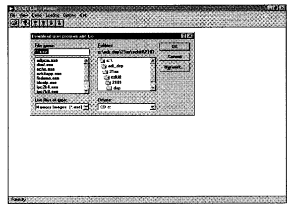
The Windows-based monitor software provided with the EZ-Kit Lite, makes it possible to load an executable file into the ADSP-2181 on the EZ-Kit Lite board. This is accomplished through the pull-down "Loading" menu by selecting "Download user program and Go" (Figure 5). This will download the filter program to the ADSP-2181 and start program execution.
Review and Preview
The goal of this article was to outline the steps from an algorithm description to a DSP executable program that could be run on a hardware development platform. Issues introduced include software development flow, architecture description, source-code generation, data I/O, and the EZ-Kit Lite hardware platform.
There are many levels of detail associated with each of these topics that this brief article could not do justice to. Further information is available in the references below. The series will continue to build on this application with additional topics. The next article will examine data input/output (I/O) issues in greater detail through the processor interrupt structure, and discuss additional features of the simple filter algorithm.
FIR Filter code listing for EZ-Kit Lite
/***************************************************************
* hello81.dsp — template file for 2181 ez-kit lite board
*
* This sample program is organized into the following sections:
*
* Assemble time constants (system.h)
* Interrupt vector table
* ADSP 2181 intialization (init1847.dsp)
* ADSP 1847 codec intialization (init1847.dsp)
* Interrupt service routines
*
* This program implements a simple ‘talk-through’ with the AD1847 codec.
* The initialization routines have been put into the init1847.dsp file. This
* file contains the interrupt vector table, the main ‘dummy’ loop, and the
* interrupt service routines for the pushbutton and the serial port 0 receive.
* The pushbutton (IRQE) causes the LED on the EZ-Kit board to toggle
* with each button press.
*
* Parameters controlling the sampling rate, gains, etc., are contained in the
* file init1847.dsp. Serial Port 0 is used to communicate with the AD1847.
* The transmit interrupts are used to configure the codec, then they are
* disabled and the receive interrupts are used to implement the ‘talk-through’
* audio.
*
* The definitions for the memory-mapped control registers are contained in
* the file: system.h
*
* The application can be built by:
*
* asm21 -c -l -2181 hello81
* asm21 -c -l -2181 init1847
* ld21 hello81 init1847 -a 2181 -e hello81 -g -x
*
**********************************************************/
.module/RAM/ABS=0 EzHello;
#include
#define taps 255 /* filter tap length */
.var/dm/circ filt_data[taps]; /* input data buffer */
.var/pm/circ filt_coeffs[taps]; /* coefficient buffer */
.init filt_coeffs:; /* initialize coefficients */
.external rx_buf, tx_buf;
.external init_cmds, stat_flag;
.external next_cmd, init_1847, init_system_regs, init_sport0;
/**********************************************************
* Interrupt vector table
**********************************************************/
jump start; rti; rti; rti; /* 00: reset */
rti; rti; rti; rti; /* 04: IRQ2 */
rti; rti; rti; rti; /* 08: IRQL1 */
rti; rti; rti; rti; /* 0c: IRQL0 */
ar = dm(stat_flag); /* 10: SPORT0 tx */
ar = pass ar;
if eq rti;
jump next_cmd;
jump input_samples; /* 14: SPORT1 rx */
rti; rti; rti;
jump irqe; rti; rti; rti; /* 18: IRQE */
rti; rti; rti; rti; /* 1c: BDMA */
rti; rti; rti; rti; /* 20: SPORT1 tx or IRQ1 */
rti; rti; rti; rti; /* 24: SPORT1 rx or IRQ0 */
rti; rti; rti; rti; /* 28: timer */
rti; rti; rti; rti; /* 2c: power down */
/************************************************************
* ADSP 2181 intialization
************************************************************/
start:
i0 = ^rx_buf; /* remember codec autobuffering uses i0 and i1 !! */
l0 = %rx_buf;
i1 = ^tx_buf;
l1 = %tx_buf;
i3 = ^init_cmds; /* i3 can be used for something else after codec init */
l3 = %init_cmds;
m0 = 0;
m1 = 1;
/* initialize serial port 0 for communication with the AD1847 codec */
call init_sport0;
/* initialize the other system registers, etc. */
call init_system_regs;
/* initialize the AD1847 codec */
call init_1847;
ifc = b#00000011111111; /* clear any pending interrupt */
nop; /* there is a 1 cycle latency for ifc */
/* setup pointers for data and coefficients */
i2 = ^filt_data;
l2 = %filt_data;
i5 = ^filt_coefs;
m5 = 1;
l5 = %filt_coefs;
imask=b#0000110000; /* enable rx0 interrupt */
/* |||||||||+ | timer
||||||||+- | SPORT1 rec or IRQ0
|||||||+-- | SPORT1 trx or IRQ1
||||||+--- | BDMA
|||||+---- | IRQE
||||+----- | SPORT0 rec
|||+------| SPORT0 trx
||+-------| IRQL0
|+--------| IRQL1
+---------| IRQ2
*/
/*----------------------------------------------------------------------
- wait for interrupt and loop forever
----------------------------------------------------------------------*/
talkthru: idle;
jump talkthru;
/**************************************************************
* Interrupt service routines
**************************************************************/
/*----------------------------------------------------------------------
- FIR Filter
----------------------------------------------------------------------*/
input_samples:
ena sec_reg; /* use shadow register bank */
ax0 = dm (rx_buf + 1); /* read data from converter */
dm(i2,m1) = ax0; /* write new data into delay line, pointer
now pointing to oldest data */
cntr = taps - 1;
mr = 0, mx0 = dm(i2,m1), my0 = pm(i5,m5); /* clear accumulator, get first
data and coefficient value */
do filt_loop until ce; /* set-up zero-overhead loop */
filt_loop: mr = mr + mx0 * my0(ss), mx0 = dm(i2,m1), my0 = pm(i5,m5);
/* MAC and two data fetches */
mr = mr + mx0 * my0 (rnd); /* final multiply, round to 16-bit result */
if mv saat mr; /* check for overflow */
dm(tx_buf+1) = mr1;
dm(tx_buf+2) = mr1; /* output data to both channels */
rti;
.endmod;
